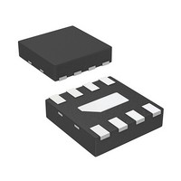
AMMP-6220-TR1 Avago Technologies US Inc., AMMP-6220-TR1 Datasheet - Page 8

AMMP-6220-TR1
Manufacturer Part Number
AMMP-6220-TR1
Description
IC MMIC LOW NOISE 6-20GHZ 8-SMD
Manufacturer
Avago Technologies US Inc.
Datasheet
1.AMMP-6220-BLK.pdf
(10 pages)
Specifications of AMMP-6220-TR1
Rf Type
ISM, MMDS, WLL, 802.16/WiMAX, DBS, VSAT
Gain
22dB
Current - Supply
55mA ~ 70mA
Frequency
6GHz ~ 20GHz
Noise Figure
2.5dB
P1db
10dBm
Package / Case
8-QFN
Voltage - Supply
3V ~ 7V
Frequency Rf
20GHz
Noise Figure Typ
2.5dB
Supply Current
55mA
Frequency Max
20GHz
Termination Type
SMD
Frequency Min
6GHz
Supply Voltage Max
3V
Manufacturer's Type
Low Noise Amplifier
Number Of Channels
1
Frequency (max)
20GHz
Operating Supply Voltage (typ)
3V
Package Type
SMT
Mounting
Surface Mount
Pin Count
8
Noise Figure (typ)
2.5dB
Filter Terminals
SMD
Rohs Compliant
Yes
Lead Free Status / RoHS Status
Lead free / RoHS Compliant
Test Frequency
-
Lead Free Status / Rohs Status
Compliant
Available stocks
Company
Part Number
Manufacturer
Quantity
Price
Company:
Part Number:
AMMP-6220-TR1
Manufacturer:
TI
Quantity:
21 557
Recommended SMT Attachment
The AMMP Packaged Devices are compatible with high
volume surface mount PCB assembly processes.
The PCB material and mounting pattern, as defined in the
data sheet, optimizes RF performance and is strongly rec-
ommended. An electronic drawing of the land pattern
is available upon request from Avago Sales & Application
Engineering.
Stencil Design Guidelines
A properly designed solder screen or stencil is required
to ensure optimum amount of solder paste is deposited
Figure 23.
Figure 24.
8
Stencil Outline Drawing (mm)
Suggested PCB Land Pattern and Stencil Layout
onto the PCB pads. The recommended stencil layout is
shown in Figure 24. The stencil has a solder paste deposi-
tion opening approximately 70% to 90% of the PCB pad.
Reducing stencil opening can potentially generate more
voids underneath. On the other hand, stencil openings
larger than 100% will lead to excessive solder paste
smear or bridging across the I/O pads. Considering the
fact that solder paste thickness will directly affect the
quality of the solder joint, a good choice is to use a laser
cut stencil composed of 0.127 mm (5 mils) thick stainless
steel which is capable of producing the required fine
stencil outline. The combined PCB and stencil layout is
shown in Figure 25.
Figure 25.
Combined PCB and Stencil Layouts


