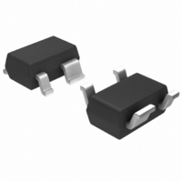
MBC13916NT1 Freescale Semiconductor, MBC13916NT1 Datasheet - Page 10

MBC13916NT1
Manufacturer Part Number
MBC13916NT1
Description
TRANS RF NPN LO NOISE SOT-343
Manufacturer
Freescale Semiconductor
Type
General Purpose Amplifierr
Specifications of MBC13916NT1
Current - Supply
20mA
Frequency
100MHz ~ 2.5GHz
Gain
16.5dB
Noise Figure
1.9dB
P1db
2.5dBm
Package / Case
SOT-343R
Rf Type
General Purpose
Test Frequency
1.9GHz
Voltage - Supply
2.7V ~ 5V
Number Of Channels
1
Operating Frequency
2500 MHz
Operating Supply Voltage
3 V
Supply Current
5.6 mA @ 2.7 V
Maximum Power Dissipation
100 mW
Maximum Operating Temperature
+ 85 C
Minimum Operating Temperature
- 40 C
Mounting Style
SMD/SMT
Technology
Low Noise Amplifier
Manufacturer's Type
Low Noise Amplifier
Frequency (max)
2.5GHz
Operating Supply Voltage (min)
2.7V
Operating Supply Voltage (typ)
3V
Operating Supply Voltage (max)
5V
Package Type
SOT-343R
Mounting
Surface Mount
Pin Count
3 +Tab
Noise Figure (typ)
2.1@1900MHzdB
Operating Temp Range
-40C to 85C
Operating Temperature Classification
Industrial
Lead Free Status / RoHS Status
Lead free / RoHS Compliant
Other names
MBC13916NT1
MBC13916NT1TR
MBC13916NT1TR
Available stocks
Company
Part Number
Manufacturer
Quantity
Price
Applications Information
Typical performance that can be expected from this circuit at 3.0 and 3.5 V V
component values can be changed to enhance the performance of a particular parameter but usually at the
expense of another. Gain can be improved by sacrificing stability (R3 and R5). Input return loss can be
sacrificed to improve noise figure. IIP3 can be improved by increasing emitter degeneration (L3) and bias
current (R2). Unused traces are available on the PCB to add emitter degeneration at leads 1 and 3 of the
device.
10
V
3.0
3.5
CC
RF In
R6
C3
V
CC
C3
(mA)
C5
5.0
6.1
I
C
C
7
Table 5. Typical 900 MHz LNA Performance
L4
Gnd
R2
Figure 19. 900 MHz LNA Board Layout
Figure 18. 900 MHz LNA Schematic
(dB)
1.21
MBC13900 Technical Data, Rev. 1.1
1.2
NF
R3
L1
R4
C1
C4
50 Ω Insertion
C2
Gain (dB)
19.7
20.2
R2
Component Value
C1
C2
C3
C4
C5
C6
L1
L2
L3
R1
R2
R3
R4
R5
R6
Vias
PCB
R3
Output IP3
(dBm)
17.6
15
1.0 µF
3.3 pF
12 pF
0.01 µF
1.0 µF
0.3 pF
6.8 nH
5.6 nH
<0.5 nH
133 Ω
49.9 kΩ
16.5 Ω
0 Ω
3.9 Ω
0 Ω
FR4
C1
V
CC
Comments
Optional Bypassing
DC Block and S
DC Block and S
Broadband bypass
Broadband bypass
IIP3 improvement
Toko LL1608-FS, match, bias
Toko LL1608-FH, match, bias
Emitter L on board (distance to GND vias)
Bias
Bias
Stability, S
Jumper
Stability, S
Jumper
D = 15 mil
ε
R5
L2
R1
r
=4.5, h=25 mil, t=1.75 mil
Input Return
Loss (dB)
C2
CC
10.1
10.8
22
22
is listed in
22
11
Freescale Semiconductor
C4
RF Out
Output Return
Loss (dB)
Table
10.2
10.8
5. The


