AD8312ACBZ-P7 Analog Devices Inc, AD8312ACBZ-P7 Datasheet - Page 2
AD8312ACBZ-P7
Manufacturer Part Number
AD8312ACBZ-P7
Description
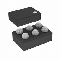
IC DETECTOR RF LOGIC 6-WLCSP
Manufacturer
Analog Devices Inc
Type
Logarithmic Amplifierr
Datasheet
1.AD8312ACBZ-P7.pdf
(20 pages)
Specifications of AD8312ACBZ-P7
Rf Type
Cellular, GSM, CDMA, W-CDMA
Frequency
50MHz ~ 3.5GHz
Input Range
-45dBm ~ 0dBm
Accuracy
±1dB
Voltage - Supply
2.7 V ~ 5.5 V
Current - Supply
5.7mA
Package / Case
6-UFBGA, 6-uCSP
Frequency Range
50MHz To 3.5GHz
Power Range
-45dBm To 0dBm
Sensitivity
0.0073dB/°C
Supply Current
4.2mA
Supply Voltage Range
2.7V To 5.5V
Rf Ic Case Style
WLCSP
Number Of Channels
1
Number Of Elements
1
Power Supply Requirement
Single
Input Resistance
0.013MOhm
Input Bias Current
75uA
Single Supply Voltage (typ)
3V
Dual Supply Voltage (typ)
Not RequiredV
Power Dissipation
200mW
Rail/rail I/o Type
No
Single Supply Voltage (min)
2.7V
Single Supply Voltage (max)
5.5V
Dual Supply Voltage (min)
Not RequiredV
Dual Supply Voltage (max)
Not RequiredV
Operating Temp Range
-40C to 85C
Operating Temperature Classification
Industrial
Mounting
Surface Mount
Pin Count
6
Package Type
WLCSP
Lead Free Status / RoHS Status
Lead free / RoHS Compliant
Lead Free Status / RoHS Status
Lead free / RoHS Compliant, Lead free / RoHS Compliant
Other names
AD8312ACBZ-P7
AD8312ACBZ-P7TR
AD8312ACBZ-P7TR
Available stocks
Company
Part Number
Manufacturer
Quantity
Price
Company:

Part Number:
AD8312ACBZ-P7
Manufacturer:
ADI
Quantity:
9 000
Company:
Part Number:
AD8312ACBZ-P7
Manufacturer:
ST
Quantity:
320


AD8312
TABLE OF CONTENTS
Specifications ..................................................................................... 3
Absolute Maximum Ratings ............................................................ 6
Pin Configuration and Function Descriptions ............................. 7
Typical Performance Characteristics ............................................. 8
General Description ....................................................................... 12
Applications ..................................................................................... 13
REVISION HISTORY
1/11—Rev. 0 to Rev. A
Changes to Figure 29 ...................................................................... 16
Updated Outline Dimensions ....................................................... 19
Changes to Ordering Guide .......................................................... 19
4/05—Revision 0: Initial Version
ESD Caution .................................................................................. 6
Basic Connections ...................................................................... 13
Transfer Function in Terms of Slope and Intercept ............... 13
Filter Capacitor ....................................................................... 14
Rev. A | Page 2 of 20
Outline Dimensions ....................................................................... 19
Ordering Guide .......................................................................... 19
Input Coupling Options ........................................................ 14
Increasing the Logarithmic Slope ........................................ 15
Effect of Waveform Type on Intercept ................................ 15
Temperature Drift .................................................................. 16
Operation Above 2.5 GHz .................................................... 16
Device Handling ..................................................................... 16
Evaluation Board .................................................................... 16
Related parts for AD8312ACBZ-P7
Image
Part Number
Description
Manufacturer
Datasheet
Request
R

Part Number:
Description:
High-Performance, Low Distortion 500-MHz Mixer
Manufacturer:
Analog Devices
Datasheet:

Part Number:
Description:
MIXER IC
Manufacturer:
Analog Devices Inc
Datasheet:
Part Number:
Description:
MIXER IC
Manufacturer:
Analog Devices Inc
Datasheet:

Part Number:
Description:
±1.7g Dual-Axis IMEMS Accelerometer Evaluation Board
Manufacturer:
Analog Devices Inc
Datasheet:

Part Number:
Description:
Inertial Sensor Evaluation System
Manufacturer:
Analog Devices Inc
Datasheet:
Part Number:
Description:
Manufacturer:
Analog Devices Inc
Datasheet:
Part Number:
Description:
Manufacturer:
Analog Devices Inc
Datasheet:
Part Number:
Description:
Manufacturer:
Analog Devices Inc
Datasheet:
Part Number:
Description:
Manufacturer:
Analog Devices Inc
Datasheet:
Part Number:
Description:
Manufacturer:
Analog Devices Inc
Datasheet:
Part Number:
Description:
Manufacturer:
Analog Devices Inc
Datasheet:
Part Number:
Description:
Manufacturer:
Analog Devices Inc
Datasheet: