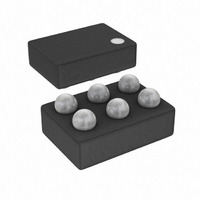
AD8312ACBZ-P7 Analog Devices Inc, AD8312ACBZ-P7 Datasheet - Page 3

AD8312ACBZ-P7
Manufacturer Part Number
AD8312ACBZ-P7
Description
IC DETECTOR RF LOGIC 6-WLCSP
Manufacturer
Analog Devices Inc
Type
Logarithmic Amplifierr
Datasheet
1.AD8312ACBZ-P7.pdf
(20 pages)
Specifications of AD8312ACBZ-P7
Rf Type
Cellular, GSM, CDMA, W-CDMA
Frequency
50MHz ~ 3.5GHz
Input Range
-45dBm ~ 0dBm
Accuracy
±1dB
Voltage - Supply
2.7 V ~ 5.5 V
Current - Supply
5.7mA
Package / Case
6-UFBGA, 6-uCSP
Frequency Range
50MHz To 3.5GHz
Power Range
-45dBm To 0dBm
Sensitivity
0.0073dB/°C
Supply Current
4.2mA
Supply Voltage Range
2.7V To 5.5V
Rf Ic Case Style
WLCSP
Number Of Channels
1
Number Of Elements
1
Power Supply Requirement
Single
Input Resistance
0.013MOhm
Input Bias Current
75uA
Single Supply Voltage (typ)
3V
Dual Supply Voltage (typ)
Not RequiredV
Power Dissipation
200mW
Rail/rail I/o Type
No
Single Supply Voltage (min)
2.7V
Single Supply Voltage (max)
5.5V
Dual Supply Voltage (min)
Not RequiredV
Dual Supply Voltage (max)
Not RequiredV
Operating Temp Range
-40C to 85C
Operating Temperature Classification
Industrial
Mounting
Surface Mount
Pin Count
6
Package Type
WLCSP
Lead Free Status / RoHS Status
Lead free / RoHS Compliant
Lead Free Status / RoHS Status
Lead free / RoHS Compliant, Lead free / RoHS Compliant
Other names
AD8312ACBZ-P7
AD8312ACBZ-P7TR
AD8312ACBZ-P7TR
Available stocks
Company
Part Number
Manufacturer
Quantity
Price
Company:
Part Number:
AD8312ACBZ-P7
Manufacturer:
ADI
Quantity:
9 000
Company:
Part Number:
AD8312ACBZ-P7
Manufacturer:
ST
Quantity:
320
SPECIFICATIONS
V
Table 1.
Parameter
SIGNAL INPUT INTERFACE
MEASUREMENT MODE
S
Specified Frequency Range
Input Voltage Range
DC Resistance to COMM
f = 50 MHz
f = 100 MHz
f = 900 MHz
= 3 V, CFLT = open, T
Equivalent Power Range
Input Impedance
±1 dB Dynamic Range
Maximum Input Level
Minimum Input Level
Slope
Intercept
Output Voltage—High Power In
Output Voltage—Low Power In
Temperature Sensitivity
Input Impedance
±1 dB Dynamic Range
Maximum Input Level
Minimum Input Level
Slope
Intercept
Output Voltage—High Power In
Output Voltage—Low Power In
Temperature Sensitivity
Input Impedance
±1 dB Dynamic Range
Maximum Input Level
Minimum Input Level
Slope
Intercept
Output Voltage—High Power In
Output Voltage—Low Power In
Temperature Sensitivity
A
= 25°C, light condition = 600 LUX, 52.3 Ω termination resistor at RFIN, unless otherwise noted.
Conditions
RFIN (Pin 6)
Internally ac-coupled
52.3 Ω external termination
VOUT (Pin 2) shorted to VSET (Pin 3), sinusoidal input signal
T
−40°C < T
±1 dB error
±1 dB error
P
P
P
25°C ≤ T
−40°C ≤ T
T
−40°C < T
±1 dB error
±1 dB error
P
P
P
25°C ≤ T
−40°C ≤ T
T
−40°C < T
±1 dB error
±1 dB error
P
P
P
25°C ≤ T
−40°C ≤ T
A
A
A
IN
IN
IN
IN
IN
IN
IN
IN
IN
= 25°C
= 25°C
= 25°C
= −10 dBm
= −40 dBm
= −10 dBm
= −10 dBm
= −40 dBm
= −10 dBm
= −10 dBm
= −40 dBm
= −10 dBm
A
A
A
A
≤ +85°C
A
A
≤ +85°C
A
A
≤ 85°C
A
< +85°C
≤ +25°C
< +85°C
≤ +25°C
< +85°C
≤ +25°C
Rev. A | Page 3 of 20
Min
0.05
1.25
−45
19.0
−56.0
Typ
100
3050 || 1.4
50
42
3
−47
20.25
−51.5
0.841
0.232
0.0010
0.0073
2900 || 1.3
48
40
2
−46
21.0
−50.5
0.850
0.222
0.0002
0.0060
890 || 1.15
49
42
1
−48.0
20.25
−51.9
0.847
0.237
0.0019
0.0010
Max
3.5
224
0
23.0
−47.0
AD8312
Unit
GHz
mV rms
dBm
kΩ
Ω || pF
dB
dB
dBm
dBm
mV/dB
dBm
V
V
dB/°C
dB/°C
Ω || pF
dB
dB
dBm
dBm
mV/dB
dBm
V
V
dB/°C
dB/°C
Ω || pF
dB
dB
dBm
dBm
mV/dB
dBm
V
V
dB/°C
dB/°C


