DEMOBOARD-T7024PGM Atmel, DEMOBOARD-T7024PGM Datasheet
DEMOBOARD-T7024PGM
Specifications of DEMOBOARD-T7024PGM


Related parts for DEMOBOARD-T7024PGM


DEMOBOARD-T7024PGM Summary of contents
Page 1
Bluetooth Front-end IC T7024 Design Guide General Information The T7024 is a single supply front-end IC especially designed for applications in the 2.4 GHz to 2.5 GHz frequency band. The front end consists of a Power Amplifier (PA), a ...
Page 2
Reference Design for PSSO20 Package Design Guide T7024 2 The typical application board that supports circuitry of the T7024 in a PSSO20 package is shown in Figure 2, Figure 3 on page 3 and Figure 4 on page 3. The ...
Page 3
Figure 3. T7024 Application Board Layout (PSSO20 Package) LNA_SUPPLY 100pF 3.9nH 100pF 1.8pF 0R LED DIL-Switch 2k7R 0R 0R 390R Figure 4. T7024 Application Board Schematic (PSSO20 Package) LNA OUT 100p * PU 100p * ...
Page 4
Reference Design for QFN20 Package Design Guide T7024 4 The typical application module support circuitry of the T7024 in a QFN20 package is shown in Figure 6 on page 5, Figure 7 on page 5 and Figure 8 on page ...
Page 5
Figure 7. T7024 Application Board Schematic (QFN20 Package) RX_ON 100p PU 100p R is selected 1 with DIL-switch PIN diode replaced by LED on application- board 4549D–BLURF–06/04 Figure 6. T7024 Application Board Layout (QFN20 Package) 0.8pF HQ LED 2k7 0R ...
Page 6
Power Amplifier Design Guide T7024 6 The power amplifier of the T7024 is designed as a three-stage amplifier. The input stage of the amplifier is AC-coupled to PA_IN. Therefore blocking capacitor is not nec- essary at the input ...
Page 7
For the design of the output matching circuit, an S-parameter test set or network ana- lyzer may not be used. The measurement of the output matching with a network analyzer results in wrong values since the measurement is done ...
Page 8
Design Guide T7024 8 Figure 8. Typical Ramp Curve for T7024 in QFN20 Package (Temperature 20° -10 -15 - 100 150 Figure 9. Schematic for Simple Temperature Compensation Power levels ...
Page 9
Low-noise Amplifier 4549D–BLURF–06/04 The Low-Noise Amplifier (LNA) of the T7024 is a two-stage amplifier with an internal matching at 2.45 GHz. The LNA includes DC supply, RF input, RF output, two control signals and ground connections. To achieve good noise ...
Page 10
Switch Driver Application Board Connectors Design Guide T7024 10 The switch driver of the T7024 front end is used to realize an antenna switch. A switched current source is used for this purpose. The supply of the LNA is also ...
Page 11
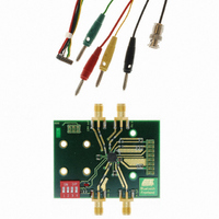
S-parameter Data for the Reference Designs 4549D–BLURF–06/04 Figure 12. LNA and PA Connectors for the Application Board LNA Connector (top view, cable leaves in top direction, upper left corner on application board) VS_LNA (red) PU (blue) Switch Out (green) RX_ON ...
Page 12
Design Guide T7024 12 Figure 14. Measured S-parameter Data for the LNA Output, QFN20 Package T7024 QFN20: LNA out 2 1 Start: 0. 050 000 000 GHz Stop: 5. 000 000 000 GHz Figure 15. Measured S-parameter Data for the ...
Page 13
Figure 16. Measured S-parameter Data for the LNA Input, PSSO20 Package T7024 PSSO20: LNA in Start: 0. 050 000 000 GHz Stop: 5. 000 000 000 GHz Figure 17. Measured S-parameter Data for the LNA Output, PSSO20 Package T7024 ...
Page 14
Load Pull Data for the Reference Designs Design Guide T7024 14 Figure 18. Measured S-parameter Data for the PA Input, PSSO20 Package T7024 PSSO20 Start: 0. 050 000 000 GHz Stop: 5. 000 000 000 ...
Page 15
Figure 19. Measured Load Impedance for the PA Output, PSSO20 Package (Reference: 50 Figure 20. Measured Load Impedance for the PA Output, QFN20 Package (Reference Design Guide T7024 15 ...
Page 16
Frequently Asked Questions Design Guide T7024 16 1. What is the advantage of SiGe Hetero Junction Transistor Technology? There are several advantages: • The silicon material itself has a 3 times higher thermal conductivity compared to GaAs material which leads ...
Page 17
Glossary 4549D–BLURF–06/04 8. What is the purpose of input and output matching? • Output matching of PA: the output of the PA device has to be matched to 50 Ohms in order to get maximum output power and efficiency. It ...
Page 18
... No licenses to patents or other intellectual property of Atmel are granted by the Company in connection with the sale of Atmel products, expressly or by implication. Atmel’s products are not authorized for use as critical components in life support devices or systems. ...