1321XEVK Freescale Semiconductor, 1321XEVK Datasheet - Page 10
1321XEVK
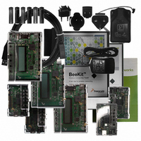
Manufacturer Part Number
1321XEVK
Description
KIT EVALUATION FOR 1321X
Manufacturer
Freescale Semiconductor
Type
Zigbeer
Specifications of 1321XEVK
Frequency
2.4GHz
Wireless Frequency
2.4 GHz
Modulation
DSSS OQPSK
Security
128 bit AES
Operating Voltage
2 VDC to 3.4 VDC
Operating Temperature Range
- 40 C to + 85 C
For Use With/related Products
MC1321x
Lead Free Status / RoHS Status
Contains lead / RoHS non-compliant


10
Pin #
19
20
21
22
23
24
25
26
27
28
29
30
31
32
33
34
35
36
37
PTC7
PTE0/TXD1
PTE1/RXD1
VDDD
VDDINT
GPIO5
GPIO6
GPIO7
XTAL1
XTAL2
VDDLO2
VDDLO1
VDDVCO
VBATT
VDDA
CT_Bias
RFIN_M
RFIN_P
NC
Pin Name
1
1
1
Digital
Input/Output
Digital
Input/Output
Digital
Input/Output
Power Output Modem regulated output
Power Input
Digital
Input/Output
Digital
Input/Output
Digital
Input/Output
Input
Input/Output
Power Input
Power Input
Power Output Modem VCO regulated
Power Input
Power Output Modem analog regulated
RF Control
Output
RF Input
(Output)
RF Input
(Output)
Type
Table 2. Pin Function Description (continued)
MC13211/212/213 Technical Data, Rev. 1.8
MCU Port C Bit 7
MCU Port E Bit 0 / SCI1 TX
data out
MCU Port E Bit 1/ SCI1 RX
data in
supply voltage
Modem digital interface
supply
General Purpose
Input/Output 5.
Modem General Purpose
Input/Output 6
Modem General Purpose
Input/Output 7
Modem crystal reference
oscillator input
Modem crystal reference
oscillator output
Modem LO2 VDD supply
Modem LO1 VDD supply
supply bypass
Modem voltage regulators’
input
supply output
Modem bias
voltage/control signal for
RF external components
Modem RF input/output
negative
Modem RF input/output
positive
Not used
Description
Decouple to ground.
2.0 to 3.4 V. Decouple to ground. Connect to
Battery.
See Footnote 1
See Footnote 1
See Footnote 1
Connect to 16 MHz crystal and load capacitor.
Connect to 16 MHz crystal and load capacitor. Do
not load this pin by using it as a 16 MHz source.
Measure 16 MHz output at CLKO, programmed for
16 MHz.
Connect to VDDA externally.
Connect to VDDA externally.
Decouple to ground.
Decouple to ground. Connect to Battery.
Decouple to ground. Connect to directly VDDLO1
and VDDLO2 externally and to PAO_P and PAO_M
through a bias network.
When used with internal T/R switch, provides
ground reference for RX and VDDA reference for
TX. Can also be used as a control signal with
external LNA, antenna switch, and/or PA (high level
is VDDA).
When used with internal T/R switch, this is a
bi-directional RF port for the internal LNA and PA
When used with internal T/R switch, this is a
bi-directional RF port for the internal LNA and PA
May be grounded or left open
Functionality
Freescale Semiconductor
Related parts for 1321XEVK
Image
Part Number
Description
Manufacturer
Datasheet
Request
R

Part Number:
Description:
Manufacturer:
Freescale Semiconductor, Inc
Datasheet:
Part Number:
Description:
Manufacturer:
Freescale Semiconductor, Inc
Datasheet:
Part Number:
Description:
Manufacturer:
Freescale Semiconductor, Inc
Datasheet:
Part Number:
Description:
Manufacturer:
Freescale Semiconductor, Inc
Datasheet:
Part Number:
Description:
Manufacturer:
Freescale Semiconductor, Inc
Datasheet:
Part Number:
Description:
Manufacturer:
Freescale Semiconductor, Inc
Datasheet:
Part Number:
Description:
Manufacturer:
Freescale Semiconductor, Inc
Datasheet:
Part Number:
Description:
Manufacturer:
Freescale Semiconductor, Inc
Datasheet:
Part Number:
Description:
Manufacturer:
Freescale Semiconductor, Inc
Datasheet:
Part Number:
Description:
Manufacturer:
Freescale Semiconductor, Inc
Datasheet:
Part Number:
Description:
Manufacturer:
Freescale Semiconductor, Inc
Datasheet:
Part Number:
Description:
Manufacturer:
Freescale Semiconductor, Inc
Datasheet:
Part Number:
Description:
Manufacturer:
Freescale Semiconductor, Inc
Datasheet:
Part Number:
Description:
Manufacturer:
Freescale Semiconductor, Inc
Datasheet:
Part Number:
Description:
Manufacturer:
Freescale Semiconductor, Inc
Datasheet: