1321XEVK Freescale Semiconductor, 1321XEVK Datasheet - Page 24
1321XEVK
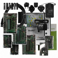
Manufacturer Part Number
1321XEVK
Description
KIT EVALUATION FOR 1321X
Manufacturer
Freescale Semiconductor
Type
Zigbeer
Specifications of 1321XEVK
Frequency
2.4GHz
Wireless Frequency
2.4 GHz
Modulation
DSSS OQPSK
Security
128 bit AES
Operating Voltage
2 VDC to 3.4 VDC
Operating Temperature Range
- 40 C to + 85 C
For Use With/related Products
MC1321x
Lead Free Status / RoHS Status
Contains lead / RoHS non-compliant


24
3.
Balun
required by the radio. Separate RFIN and PAO signals are provided for connection with the baluns,
and the CT_Bias signal is programmed to provide the external switch control. The polarity of the
external switch control is selectable.
Figure 14C
the receive side, the RX antenna is ac-coupled to the differential RFIN inputs and these capacitors
along with inductor L1 form a matching network. Inductors L2 and L3 are ac-coupled to ground to
form a frequency trap. For the transmit side, the TX antenna is connected to the differential PAO
outputs, and inductors L4 and L5 provide dc-biasing to VDDA but are ac isolated.
14A) Using Onboard T/R Switch
Bypass
shows a dual antenna configuration where there is a RX antenna and a TX antenna. For
L1
Figure 14. Using the MC1321x with External RF Components
PAO_M
RFIN_M (PAO_M)
PAO_P
RFIN_P (PAO_P)
CT_Bias
RX Antenna
TX Antenna
L1
MC1321x
MC13211/212/213 Technical Data, Rev. 1.8
Bypass
L2
L4
14C) Using Dual Antennae
VDDA
L3
L5
Bypass
A nt
S w
14B) Using External Antenna Switch With LNA
RFIN_P (PAO_P)
PAO_M
RFIN_M (PAO_M)
CT_Bias
PAO_P
V D D
L NA
MC1321x
B a lun
B a lun
B yp a ss
B yp a s s
V D D A
Freescale Semiconductor
L 1
R F IN _ M (P A O _ M )
P A O _ M
P A O _ P
RF IN_ P (P A O _ P )
(A nt S w C tl)
C T_ B ia s
M C 1321x
Related parts for 1321XEVK
Image
Part Number
Description
Manufacturer
Datasheet
Request
R

Part Number:
Description:
Manufacturer:
Freescale Semiconductor, Inc
Datasheet:
Part Number:
Description:
Manufacturer:
Freescale Semiconductor, Inc
Datasheet:
Part Number:
Description:
Manufacturer:
Freescale Semiconductor, Inc
Datasheet:
Part Number:
Description:
Manufacturer:
Freescale Semiconductor, Inc
Datasheet:
Part Number:
Description:
Manufacturer:
Freescale Semiconductor, Inc
Datasheet:
Part Number:
Description:
Manufacturer:
Freescale Semiconductor, Inc
Datasheet:
Part Number:
Description:
Manufacturer:
Freescale Semiconductor, Inc
Datasheet:
Part Number:
Description:
Manufacturer:
Freescale Semiconductor, Inc
Datasheet:
Part Number:
Description:
Manufacturer:
Freescale Semiconductor, Inc
Datasheet:
Part Number:
Description:
Manufacturer:
Freescale Semiconductor, Inc
Datasheet:
Part Number:
Description:
Manufacturer:
Freescale Semiconductor, Inc
Datasheet:
Part Number:
Description:
Manufacturer:
Freescale Semiconductor, Inc
Datasheet:
Part Number:
Description:
Manufacturer:
Freescale Semiconductor, Inc
Datasheet:
Part Number:
Description:
Manufacturer:
Freescale Semiconductor, Inc
Datasheet:
Part Number:
Description:
Manufacturer:
Freescale Semiconductor, Inc
Datasheet: