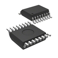
MICRF211AYQS Micrel Inc, MICRF211AYQS Datasheet - Page 6

MICRF211AYQS
Manufacturer Part Number
MICRF211AYQS
Description
IC RX 3V 380-450 MHZ 16-QSOP
Manufacturer
Micrel Inc
Specifications of MICRF211AYQS
Operating Temperature
-40°C ~ 105°C
Frequency
380MHz ~ 450MHz
Sensitivity
-110dBm
Data Rate - Maximum
10 kbps
Modulation Or Protocol
ASK, OOK
Applications
ISM, Garage Door Openers, RKE
Current - Receiving
6mA
Data Interface
PCB, Surface Mount
Antenna Connector
PCB, Surface Mount
Features
No IF Filter Required
Voltage - Supply
3 V ~ 3.6 V
Package / Case
16-QSOP
Data Rate
1Kbps
Frequency Range
380MHz To 450MHz
Modulation Type
ASK, OOK
Sensitivity Dbm
-110dBm
Rf Ic Case Style
QSOP
No. Of Pins
16
Supply Voltage Range
3V To 3.6V
Operating Frequency (max)
450000kHz
Operating Temperature (min)
-40C
Operating Temperature (max)
105C
Operating Temperature Classification
Industrial
Operating Supply Voltage (typ)
3.3V
Operating Supply Voltage (max)
3.6V
Lead Free Status / RoHS Status
Lead free / RoHS Compliant
Memory Size
-
Lead Free Status / Rohs Status
Compliant
Other names
576-1964-5
MICRF211AYQS
MICRF211AYQS
Available stocks
Company
Part Number
Manufacturer
Quantity
Price
Part Number:
MICRF211AYQS-TR
Manufacturer:
MICROCHIP/微芯
Quantity:
20 000
March 2007
Micrel
Functional Diagram
Functional Description
Figure 1. Simplified Block Diagram that illustrates the
basic structure of the MICRF211. It is made of three
sub-blocks; Image Rejection UHF Down-converter, the
OOK Demodulator, and Reference and Control Logics.
Outside the device, the MICRF211 requires only three
components to operate: two capacitors (CTH, and
CAGC) and the reference frequency device, usually a
quartz crystal. An additional five components may be
used to improve performance. These are: power supply
decoupling capacitor, two components for the matching
network, and two components for the pre-selector band
pass filter.
Receiver Operation
LNA
The RF input signal is AC-coupled into the gate circuit of
the grounded source LNA input stage. The LNA is a
Cascoded NMOS.
Mixers and Synthesizer
The LO ports of the Mixers are driven by quadrature
local oscillator outputs from the synthesizer block. The
local oscillator signal from the synthesizer is placed on
the low side of the desired RF signal to allow
suppression of the image frequency at twice the IF
frequency below the wanted signal. The local oscillator
Figure 1. Simplified Block Diagram.
6
is set to 32 times the crystal reference frequency via a
phase-locked loop synthesizer with a fully integrated
loop filter.
Image Reject Filter and Band-Pass Filter
The IF ports of the mixer produce quadrature down
converted IF signals. These IF signals are low-pass
filtered to remove higher frequency products prior to the
image reject filter where they are combined to reject the
image frequencies. The IF signal then passes through a
third order band pass filter. The IF center frequency is
1.2MHz. The IF BW is 330kHz @ 433.92MHz, and this
varies with RF operating frequency. The IF BW can be
calculated via direct scaling:
BW
These filters are fully integrated inside the MICRF211.
After filtering, four active gain controlled amplifier stages
enhance the IF signal to proper level for demodulation.
OOK Demodulator
The demodulator section is comprised of detector,
programmable
comparator.
Detector and Programmable Low-Pass Filter
The demodulation starts with the detector removing the
IF
= BW
IF@433.92 MHz
low
pass
×
⎛
⎜
⎝
Operating
filter,
433.92
slicer,
Freq
(408) 944-0800
M9999-030107
(MHz)
MICRF211
and
⎞
⎟
⎠
AGC


