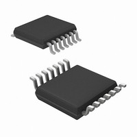
MRF49XA-I/ST Microchip Technology, MRF49XA-I/ST Datasheet - Page 46

MRF49XA-I/ST
Manufacturer Part Number
MRF49XA-I/ST
Description
IC RF TXRX 433/868/915 16-TSSOP
Manufacturer
Microchip Technology
Datasheet
1.MRF49XA-IST.pdf
(102 pages)
Specifications of MRF49XA-I/ST
Package / Case
16-TSSOP
Frequency
433MHz, 868MHz, 915MHz
Data Rate - Maximum
256kbps
Modulation Or Protocol
FHSS, FSK
Applications
Home / Industrial Automation, Remote Access, Security Alarms
Power - Output
7dbm
Sensitivity
-110dBm
Voltage - Supply
2.2 V ~ 3.8 V
Current - Receiving
11mA
Current - Transmitting
15mA
Data Interface
PCB, Surface Mount
Antenna Connector
PCB, Surface Mount
Operating Temperature
-40°C ~ 85°C
Number Of Receivers
1
Number Of Transmitters
2
Wireless Frequency
433 MHz to 915 MHz
Output Power
+ 7 dBm
Operating Supply Voltage
2.5 V, 3.3 V
Maximum Operating Temperature
+ 85 C
Mounting Style
SMD/SMT
Minimum Operating Temperature
- 40 C
Modulation
FHSS, FSK
Lead Free Status / RoHS Status
Lead free / RoHS Compliant
Memory Size
-
Lead Free Status / Rohs Status
Lead free / RoHS Compliant
Other names
579-MRF49XA-1/ST
Available stocks
Company
Part Number
Manufacturer
Quantity
Price
Company:
Part Number:
MRF49XA-I/ST
Manufacturer:
IR
Quantity:
450
Part Number:
MRF49XA-I/ST
Manufacturer:
MICROCHIP/微芯
Quantity:
20 000
3.1.2
Spikes or glitches are found on the V
supply filtering is not satisfactory, or the internal resis-
tance of the power supply is very high. So, in this case,
the Sensitive Reset mode needs to be enabled. Here,
the device Reset occurs due to the transients present
on the V
The internal Reset block has two basic modes of
operation:
• Sensitive Reset Mode
• Normal Reset Mode
Sensitive Reset Mode: By enabling the Sensitive
Reset, a Reset is generated if:
• the positive going edge of the V
• the voltage difference between the internal ramp
The Sensitive Reset mode is the default mode which
can be changed by using the DRSTM bit (FIFOR-
STREG<0>). Figure 3-2 shows the Sensitive Reset
mode.
FIGURE 3-2:
DS70590B-page 44
MRF49XA
rate greater than 100 mV/ms, and
signal and the V
voltage (600 mV).
(Pin 10)
RESET
Output
DD
line.
POWER GLITCH RESET
1.6V
V
H
L
DD
DD
reaches the Reset threshold
SENSITIVE RESET ENABLED
DD
DD
has a rising
line if the power
Voltage (600 m V)
Reset Threshold
Preliminary
Normal Reset Mode: The device enters this mode,
when the power glitch detection circuit is disabled.
Figure 3-3 shows the Normal Reset mode.
If the Sensitive mode is disabled and the power supply
is turned off, the V
Power-on Reset when the supply voltage is reapplied.
If the decoupling capacitors retain their charges for a
longer duration, there might be no Reset after
power-up as the power glitch detector is disabled.
Note:
Note:
Negative change in the supply voltage
does not cause a Reset event unless the
V
voltage (i.e., 250 mV in Normal Reset
mode, 1.6V in Sensitive Reset mode).
The Reset event reinitializes the internal
registers, and thus, the Sensitive mode is
enabled again.
DD
level reaches the Reset threshold
DD
© 2009 Microchip Technology Inc.
requires 250 mV to trigger a
Reset Ram p Line
(100 m V/m s)
Tim e


