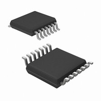
MRF49XA-I/ST Microchip Technology, MRF49XA-I/ST Datasheet - Page 53

MRF49XA-I/ST
Manufacturer Part Number
MRF49XA-I/ST
Description
IC RF TXRX 433/868/915 16-TSSOP
Manufacturer
Microchip Technology
Datasheet
1.MRF49XA-IST.pdf
(102 pages)
Specifications of MRF49XA-I/ST
Package / Case
16-TSSOP
Frequency
433MHz, 868MHz, 915MHz
Data Rate - Maximum
256kbps
Modulation Or Protocol
FHSS, FSK
Applications
Home / Industrial Automation, Remote Access, Security Alarms
Power - Output
7dbm
Sensitivity
-110dBm
Voltage - Supply
2.2 V ~ 3.8 V
Current - Receiving
11mA
Current - Transmitting
15mA
Data Interface
PCB, Surface Mount
Antenna Connector
PCB, Surface Mount
Operating Temperature
-40°C ~ 85°C
Number Of Receivers
1
Number Of Transmitters
2
Wireless Frequency
433 MHz to 915 MHz
Output Power
+ 7 dBm
Operating Supply Voltage
2.5 V, 3.3 V
Maximum Operating Temperature
+ 85 C
Mounting Style
SMD/SMT
Minimum Operating Temperature
- 40 C
Modulation
FHSS, FSK
Lead Free Status / RoHS Status
Lead free / RoHS Compliant
Memory Size
-
Lead Free Status / Rohs Status
Lead free / RoHS Compliant
Other names
579-MRF49XA-1/ST
Available stocks
Company
Part Number
Manufacturer
Quantity
Price
Company:
Part Number:
MRF49XA-I/ST
Manufacturer:
IR
Quantity:
450
Part Number:
MRF49XA-I/ST
Manufacturer:
MICROCHIP/微芯
Quantity:
20 000
3.8
Certain control register values must be initialized for
the basic operations of MRF49XA. These values differ
from the Power-on Reset values and provide improved
operational parameters. These settings are normally
made once after a Reset. After initialization, the
MRF49XA device features can be configured for the
application. Here, accessing a register is implied as a
command to the MRF49XA device through the SPI
port. The steps to be followed for the initialization of
MRF49XA using the control registers are as follows:
1.
2.
3.
4.
5.
6.
7.
8.
9.
10. Tune in the antenna.
11. Turn off the transmitter and turn on the receiver.
12. Enable FIFO for data reception.
13. Set FIFORSTREG.
14. Enable synchronous latch from FIFORSTREG.
15. Read STSREG.
The following steps should be followed to tune in the
antenna section:
1.
2.
The registers associated with initialization are:
• STSREG (see Register 2-1)
• GENCREG (see Register 2-2)
• AFCCREG (see Register 2-3)
• TXCREG (see Register 2-4)
• CFSREG (see Register 2-6)
• RXCREG (see Register 2-7)
• FIFORSTREG (see Register 2-10)
• DRSREG (see Register 2-12)
• PMCREG (see Register 2-13)
© 2009 Microchip Technology Inc.
Set FIFORSTREG.
Enable synchronous latch from FIFORSTREG.
Program frequency band and crystal load
capacitance from GENCREG.
Enable AFC function from AFCCREG.
Set center frequency through CFSREG for
transmit or receive frequency.
Set data rate through DRSREG.
Enable required functions (transmit, receive,
etc.) from PMCREG.
Configure RXCREG.
Configure TXCREG.
Turn on the transmitter section from PMCREG.
Wait for 5 ms for the oscillator to get stabilized.
Initialization
Preliminary
3.9
The advanced interrupt handler circuit is implemented
in the MRF49XA to reduce the power consumption. As
mentioned, the Sleep mode is the lowest power
consumption mode in which the mode clock and all
functional blocks of the chip are disabled. However, the
WUT and LBD circuits can be active if enabled. In case
of any interrupt, the device wakes up, switches to the
Active mode and an interrupt signal generated on the
IRO pin of the device indicates the change in state or
occurrence of an interrupt to the host microcontroller.
The source of the interrupt is determined by reading the
status word of the device (see Register 2-1).
The receiver generates an active-low interrupt request
for the microcontroller at the following events:
• TXBREG is ready to receive the next byte
• RXFIFOREG has received the preprogrammed
• RXFIFOREG overflow/TXBREG underrun
• Negative pulse on Interrupt Input pin (INT)
• Wake-up Timer Time-out (WUTINT)
• Supply voltage below the preprogrammed value is
• Power-on Reset
amount of bits
detected
Interrupts
MRF49XA
DS70590B-page 51


