MRF49XA-I/ST Microchip Technology, MRF49XA-I/ST Datasheet - Page 48
MRF49XA-I/ST
Manufacturer Part Number
MRF49XA-I/ST
Description
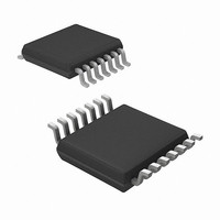
IC RF TXRX 433/868/915 16-TSSOP
Manufacturer
Microchip Technology
Datasheet
1.MRF49XA-IST.pdf
(102 pages)
Specifications of MRF49XA-I/ST
Package / Case
16-TSSOP
Frequency
433MHz, 868MHz, 915MHz
Data Rate - Maximum
256kbps
Modulation Or Protocol
FHSS, FSK
Applications
Home / Industrial Automation, Remote Access, Security Alarms
Power - Output
7dbm
Sensitivity
-110dBm
Voltage - Supply
2.2 V ~ 3.8 V
Current - Receiving
11mA
Current - Transmitting
15mA
Data Interface
PCB, Surface Mount
Antenna Connector
PCB, Surface Mount
Operating Temperature
-40°C ~ 85°C
Number Of Receivers
1
Number Of Transmitters
2
Wireless Frequency
433 MHz to 915 MHz
Output Power
+ 7 dBm
Operating Supply Voltage
2.5 V, 3.3 V
Maximum Operating Temperature
+ 85 C
Mounting Style
SMD/SMT
Minimum Operating Temperature
- 40 C
Modulation
FHSS, FSK
Lead Free Status / RoHS Status
Lead free / RoHS Compliant
Memory Size
-
Lead Free Status / Rohs Status
Lead free / RoHS Compliant
Other names
579-MRF49XA-1/ST
Available stocks
Company
Part Number
Manufacturer
Quantity
Price
Company:

Part Number:
MRF49XA-I/ST
Manufacturer:
IR
Quantity:
450
Part Number:
MRF49XA-I/ST
Manufacturer:
MICROCHIP/微芯
Quantity:
20 000


selecting the right crystal.
3.3
The power amplifier is an open-collector, differential
output with programmable output power which can
directly drive a loop or dipole antenna, and with proper
matching, can also drive a monopole antenna. An auto-
matic antenna tuning circuit configured in the power
amplifier avoids the manual tuning during production
and this offsets “hand effects”.
The registers associated with the power amplifier are:
• TXCREG (see Register 2-4)
• PMCREG (see Register 2-13)
The input LNA has selectable gain (0 dB, -6 dB, -14 dB
and -20 dB) which is useful in environments with strong
interferers. The LNA has 250Ω of differential input
impedance, which requires a matching circuit when
connected to 50Ω devices.
The registers associated with the Low Noise Amplifier
are:
• RXCREG (see Register 2-7)
• PMCREG (see Register 2-13)
3.4
The MRF49XA has a single pin crystal oscillator circuit,
which provides a 10 MHz reference signal for the
on-chip PLL. The clock frequency is programmable from
eight predefined frequencies, each being a prescaled
value of a 10 MHz crystal reference. A programmable
crystal load capacitor has been internally configured to
reduce the external component count and to have a
much simplified design. The internal load capacitor is
programmable from 8.5 pF to 16 pF in 0.5 pF steps. This
provides the advantage of accepting a wide range of
crystals from different manufacturers with different load
capacitance requirements. For load capacitance values,
see Table 3-1. These values are programmable through
the BCSREG (see Register 2-16).
The crystal oscillator circuit is sensitive to parasitic
capacitance for start-up. A small amount of parasitic
capacitance is needed to facilitate oscillation. To achieve
this, create a ground plane around the crystal and widen
the connection to the MRF49XA. This is to adjust the ref-
erence frequency and to compensate for stray capaci-
tance that might be introduced due to PCB layout. If the
layout is not possible, a 0.5-1 pF capacitor, soldered
across the crystal, will initiate the start-up. Also, see
Section 3.6 “Crystal Selection Guidelines” for
DS70590B-page 46
MRF49XA
Power and Low Noise Amplifiers
Crystal Oscillator and Clock
Output
Preliminary
TABLE 3-1:
The crystal oscillator provides a reference signal to the
RF synthesizer, baseband circuits and digital signal
processing parts. If receiver or transmitter blocks are
used frequently, it is recommended to leave the
oscillator running because the crystal might need a few
milliseconds to start and stabilize. The stabilization
time mainly depends on the crystal parameters.
The CLKOEN bit (PMCREG<0>) is used to enable or
disable the clock output.
3.4.1
The MRF49XA provides the clock signal for the micro-
controller for accurate timing, and thus, removes the
need for a second crystal for any board design. When
the microcontroller turns off the crystal oscillator by
clearing the OSCEN bit (PMCREG<3>), the MRF49XA
provides a fixed number (192) of further clock pulses for
the microcontroller to switch itself to Idle or Sleep mode
(Low-Power Consumption modes). To use this feature,
STSREG must be read before the OSCEN bit is set to
‘0’. If STSREG is not read, then the clock output will not
shut down. If the CLKOUT pin is not used, it is suggested
to turn off the output buffer from PMCREG.
The microcontroller clock source (if the clock is not sup-
plied by the MRF49XA) should be stable enough over
temperature and voltage ranges to ensure a minimum
of 16 bits time delay under all operating circumstances.
CAP3
Note:
0
0
0
0
0
0
0
0
1
1
1
1
1
1
1
1
CAP2
CLOCK TAIL FEATURE
Leaving blocks needlessly turned on
increases the current consumption, and
thus, reduces the battery life.
0
0
0
0
1
1
1
1
0
0
0
0
1
1
1
1
PROGRAMMABLE LOAD
CAPACITANCE VALUE
CAP1
© 2009 Microchip Technology Inc.
0
0
1
1
0
0
1
1
0
0
1
1
0
0
1
1
CAP0
0
1
0
1
0
1
0
1
0
1
0
1
0
1
0
1
Capacitance
Load
10.5
12.5
13.5
14.5
15.5
11.5
8.5
9.5
10
11
12
13
14
15
16
9
Related parts for MRF49XA-I/ST
Image
Part Number
Description
Manufacturer
Datasheet
Request
R

Part Number:
Description:
Manufacturer:
Microchip Technology Inc.
Datasheet:
Part Number:
Description:
Manufacturer:
Microchip Technology Inc.
Datasheet:
Part Number:
Description:
Manufacturer:
Microchip Technology Inc.
Datasheet:
Part Number:
Description:
Manufacturer:
Microchip Technology Inc.
Datasheet:
Part Number:
Description:
Manufacturer:
Microchip Technology Inc.
Datasheet:
Part Number:
Description:
Manufacturer:
Microchip Technology Inc.
Datasheet:
Part Number:
Description:
Manufacturer:
Microchip Technology Inc.
Datasheet:
Part Number:
Description:
Manufacturer:
Microchip Technology Inc.
Datasheet:
Part Number:
Description:
Manufacturer:
Microchip Technology Inc.
Datasheet: