LMX9830SM/NOPB National Semiconductor, LMX9830SM/NOPB Datasheet - Page 6
LMX9830SM/NOPB
Manufacturer Part Number
LMX9830SM/NOPB
Description
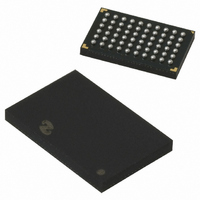
IC SRL PORT MOD BLUETOOTH 60FBGA
Manufacturer
National Semiconductor
Datasheet
1.LMX9830SMNOPB.pdf
(46 pages)
Specifications of LMX9830SM/NOPB
Frequency
2.4GHz
Data Rate - Maximum
704kbps
Modulation Or Protocol
Bluetooth v2.0, Class 2
Applications
PDA's, POS Terminals
Power - Output
0dBm
Sensitivity
-80dBm
Voltage - Supply
2.5 V ~ 3.6 V
Current - Receiving
65mA
Current - Transmitting
65mA
Data Interface
PCB, Surface Mount
Antenna Connector
PCB, Surface Mount
Operating Temperature
-40°C ~ 125°C
Package / Case
60-FBGA
Physical Interfaces
UART
Data Rate
704Kbps
Operating Temperature Range
-40°C To +125°C
Msl
MSL 4 - 72 Hours
Supply Voltage Range
1.6V To 3.6V
Frequency Max
2480MHz
Termination Type
SMD
Rohs Compliant
Yes
Filter Terminals
SMD
Frequency Min
2402MHz
Lead Free Status / RoHS Status
Lead free / RoHS Compliant
Memory Size
-
Lead Free Status / Rohs Status
Compliant
Other names
*LMX9830SM
*LMX9830SM/NOPB
LMX9830SM
*LMX9830SM/NOPB
LMX9830SM


www.national.com
I
I
I
I
I
I
I
V
V
V
I
I
RX
P
IMP
(Note 14), (Note 15)
RSSI
CC-TX
CC-RX
RXSL
RXM
SnM
SC-TLDIS
Idle
OH
OL
IH
IL
HYS
in
Symbol
Note 8: Power supply requirements based on Class II output power.
Note 9: Based on UART Baudrate 921.6 kbit/s.
Note 10: V
Note 11: Average values excluding IO.
8.1 DC CHARACTERISTICS
Note 12: Guaranteed by design.
8.2 RF PERFORMANCE CHARACTERISTICS
In the performance characteristics tables the following applies:
•
•
•
•
RF system performance specifications are guaranteed on National Semiconductor Mesa Board rev 1.1 reference design platform.
RF
sense
Symbol
All tests performed are based on Bluetooth Test Specification revision 2.0.
All tests are measured at antenna port unless otherwise specified
T
VDD_RF = 2.8V unless otherwise specified.
A
Symbol
= -40°C to +85°C
CC
Logical 1 Input Voltage high
(except oscillator I/O)
Logical 0 Input Voltage low
(except oscillator I/O)
Hysteresis Loop Width (Note 12)
Logical 1 Output Current
Logical 0 Output Current
= 3.3V, VCC_IO = 3.3V, Ambient Temperature = +25°C.
Power supply current for continuous transmit
Power supply current for continuous receive
Receive Data in SPP Link, Slave (Note 11)
Receive Data in SPP Link, Master (Note 11)
Sniff Mode, Sniff interval 1 second (Note 11)
Scanning, No Active Link, TL Disabled (Note 11)
Idle, Scanning Disabled, TL Disabled (Note 11)
Receive Sensitivity
Maximum Input Level
Intermodulation Performance F1= + 3 MHz,
RSSI Dynamic Range at LNA
Input
Parameter
Parameter
TABLE 4. Power Supply Requirements (Notes 8, 9)
TABLE 6. Receiver Performance Characteristics
Parameter
TABLE 5. Digital DC Characteristics
1.6V
3.0V
1.6V
3.0V
V
VCC_IO = 3.0V
V
VCC_IO = 3.0V
OH
OH
BER < 0.001
F2= + 6 MHz,
P
= 2.4V,
= 0.4V,
in
≤
≤
≤
≤
RF = -64 dBm
VCC_IO
VCC_IO
VCC_IO
VCC_IO
Condition
6
≤
≤
≤
≤
Condition
3.0V
3.6V
3.0V
3.6V
2.402 GHz
2.441 GHz
2.480 GHz
0.7 x VCC_IO
0.1 x VCC_IO
Min
Min
-0.2
-0.2
-10
10
2
(Note 10)
Min
-10
-38
-72
0.43
Typ
100
5.6
26
23
0.25 x VCC_IO
VCC_IO + 0.2
VCC_IO + 0.2
(Note 13)
Typ
-80
-80
-80
-36
Max
0
0.8
Max
65
65
Max
-76
-76
-76
-52
Units
Unit
mA
mA
mA
mA
mA
mA
mA
mA
dBm
dBm
dBm
dBm
dBm
dBm
µA
Unit
V
V
V
Related parts for LMX9830SM/NOPB
Image
Part Number
Description
Manufacturer
Datasheet
Request
R

Part Number:
Description:
Manufacturer:
National Semiconductor
Datasheet:

Part Number:
Description:
National Semiconductor [8-Bit D/A Converter]
Manufacturer:
National Semiconductor
Datasheet:
Part Number:
Description:
National Semiconductor [Media Coprocessor]
Manufacturer:
National Semiconductor
Datasheet:
Part Number:
Description:
Digitally Controlled Tone and Volume Circuit with Stereo Audio Power Amplifier, Microphone Preamp Stage and National 3D Sound
Manufacturer:
National Semiconductor
Datasheet:
Part Number:
Description:
Digitally Controlled Tone and Volume Circuit with Stereo Audio Power Amplifier, Microphone Preamp Stage and National 3D Sound
Manufacturer:
National Semiconductor
Datasheet:
Part Number:
Description:
AC97 Rev 2 Codec with Sample Rate Conversion and National 3D Sound
Manufacturer:
National Semiconductor
Part Number:
Description:
Manufacturer:
National Semiconductor
Datasheet:
Part Number:
Description:
Manufacturer:
National Semiconductor
Datasheet:
Part Number:
Description:
General Purpose, Low Voltage, Low Power, Rail-to-Rail Output Operational Amplifiers
Manufacturer:
National Semiconductor
Datasheet:
Part Number:
Description:
8-bit 20 MSPS flash A/D converter.
Manufacturer:
National Semiconductor
Datasheet:
Part Number:
Description:
Low Noise Quad Operational Amplifier
Manufacturer:
National Semiconductor
Datasheet:
Part Number:
Description:
Quad Differential Line Receivers
Manufacturer:
National Semiconductor
Datasheet:
Part Number:
Description:
Quad High Speed Trapezoidal? Bus Transceiver
Manufacturer:
National Semiconductor
Datasheet:
Part Number:
Description:
Dual Line Receiver
Manufacturer:
National Semiconductor
Datasheet: