STEVAL-TDR028V1 STMicroelectronics, STEVAL-TDR028V1 Datasheet - Page 6
STEVAL-TDR028V1
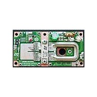
Manufacturer Part Number
STEVAL-TDR028V1
Description
BOARD DEMO RF PWR AMP STAC2942B
Manufacturer
STMicroelectronics
Type
Power Amplifierr
Specifications of STEVAL-TDR028V1
Contents
Board
Maximum Operating Temperature
+ 70 C
Operating Supply Voltage
48 V
Product
Power Management Development Tools
For Use With/related Products
STAC2942B
Lead Free Status / RoHS Status
Lead free / RoHS Compliant
Other names
497-10763


STAC2942B mounting recommendations
4.3
4.4
4.5
6/11
Surface conditions of the mounting base
The mounting base, or surface of the heatsink to which the backside of the package is
mounted, must be flat, clean, and free of tool marks.
●
●
Flatness and roughness values can be achieved on the above-mentioned materials with
standard machining processes, such as milling.
Holes for screws, solder wells, etc. should be slightly countersunk and/or de-burred.
Thermal interface material
Careful consideration must be paid to the actual interface layer between the backside of the
package and the mounting base. Cleanliness is key: particulates, grease, and oxidation
should be removed using standard practices.
A thermal interface material (TIM) of good thermal conductivity should be used in order to fill
any discontinuities between the package and mounting base surface. The decision of which
TIM material to use is based on many factors. Many types of TIMs are available today with
an incredible range of thermal/electrical/mechanical properties. Several are listed here:
●
●
●
●
●
In all cases, the chosen TIM should be no thicker than necessary and applied as evenly as
possible. For liquid compounds, it is easiest to apply to the backside of the package, keeping
in mind that excessive TIM thickness results in a higher thermal resistance than using no
TIM at all. For foils and soldering it is best to specify an appropriately-sized “preform” and
apply it to the thermal base.
Seating plane
The seating plane refers to the distance between the thermal base and the bottom of the
transistor leads. This is shown on the package outline drawing to indicate the total thickness
of the PCB, or PCB+channel depth of the heatsink. Some points to consider are:
●
Flatness: 400 µin/in (0.4 µm/mm)
Roughness: Ra<30 µin (0.8 µm)
WPSII (a silicone-free compound, Austerlitz Electronics),
Type 340 (Dow Corning)
Type 120 (a silicone compound, Wakefield Thermal Solutions)
Indium foil (Indium Corp.)
Sn63Pb37 or Pb-free solder
The leads of the transistor should launch perpendicular to the package body onto the
traces of the PCB to reduce mechanical stress to the package and solder joints. In
some cases, the PCB fabrication tolerances are such that the leads extend above the
plane defined by the top of the PCB; this situation is best handled with a judicious
selection of solder pad preform or paste thickness, or by a slight downward bending of
the transistor leads (no more than 0.01 in (0.25 mm). In no case should the leads be
Doc ID 17469 Rev 1
STEVAL-TDR028V1
Related parts for STEVAL-TDR028V1
Image
Part Number
Description
Manufacturer
Datasheet
Request
R

Part Number:
Description:
BOARD EVAL FOR ST802RT1
Manufacturer:
STMicroelectronics
Datasheet:

Part Number:
Description:
EVAL BOARD 100 BASE T
Manufacturer:
STMicroelectronics
Datasheet:

Part Number:
Description:
BOARD ELECT FISCAL CASH REGISTER
Manufacturer:
STMicroelectronics
Datasheet:
Part Number:
Description:
BOARD EVAL FOR ST802RT1A
Manufacturer:
STMicroelectronics
Datasheet:

Part Number:
Description:
2 kW/100 V RF demonstration board for 3 T MRI based on the STAC4932B
Manufacturer:
STMICROELECTRONICS [STMicroelectronics]
Datasheet:

Part Number:
Description:
BOARD EVAL FOR MEMS SENSORS
Manufacturer:
STMicroelectronics
Datasheet:
Part Number:
Description:
EVALBOARD/STEVAL-ISV014V1
Manufacturer:
STMicroelectronics

Part Number:
Description:
BOARD EVAL FOR VACUUM CLEANER
Manufacturer:
STMicroelectronics
Datasheet:

Part Number:
Description:
KIT DEV STARTER ST10F276Z5
Manufacturer:
STMicroelectronics
Datasheet:

Part Number:
Description:
BOARD LED CTLR/DVR STLED316S
Manufacturer:
STMicroelectronics
Datasheet:
Part Number:
Description:
STMicroelectronics [RIPPLE-CARRY BINARY COUNTER/DIVIDERS]
Manufacturer:
STMicroelectronics
Datasheet:
Part Number:
Description:
STMicroelectronics [LIQUID-CRYSTAL DISPLAY DRIVERS]
Manufacturer:
STMicroelectronics
Datasheet:
Part Number:
Description:
BOARD EVAL FOR MEMS SENSORS
Manufacturer:
STMicroelectronics
Datasheet: