AT88RF1354-ZU Atmel, AT88RF1354-ZU Datasheet - Page 33
AT88RF1354-ZU
Manufacturer Part Number
AT88RF1354-ZU
Description
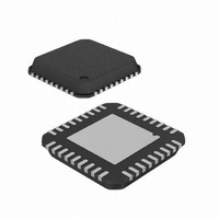
IC RF READER 13.56MHZ 36-VQFN
Manufacturer
Atmel
Datasheet
1.AT88RF1354-ZU.pdf
(48 pages)
Specifications of AT88RF1354-ZU
Frequency
13.56MHz
Features
ISO14443-B
Package / Case
36-VQFN Exposed Pad, 36-HVQFN, 36-SQFN, 36-DHVQFN
Pin Count
36
Screening Level
Industrial
Lead Free Status / RoHS Status
Lead free / RoHS Compliant
Rf Type
-
Lead Free Status / Rohs Status
Compliant


Appendix D. QFN Package Mounting Guidelines
D.1.
D.2.
8547B–RFID–3/09
Introduction
This Appendix provides PCB designers with a set of guidelines for successful board mounting of Atmel’s QFN
MicroLeadFrame ® package. The QFN package is a near chip scale plastic encapsulated package with a copper
leadframe substrate. This is a leadless package where electrical contact to the PCB is made by soldering the lands on
the bottom surface of the package to the PCB, instead of the conventional formed perimeter leads. The ePad
technology enhances the thermal and electrical properties of the package. The exposed die attach paddle on the
bottom efficiently conducts heat to the PCB and provides a stable ground through down bonds and electrical
connections through conductive die attach material.
Surface Mount Considerations for QFN Packages
For devices to perform at their peak, special considerations are needed to properly design the board and to mount the
package. For enhanced thermal, electrical, and board level performance, the exposed pad on the package needs to be
soldered to the board using a corresponding thermal pad on the board. Furthermore, for proper heat conduction
through the board, thermal vias need to be incorporated in the PCB in the thermal pad region. The PCB footprint
design needs to be considered from dimensional tolerances due to the package, PCB, and the assembly factors. A
number of factors may have a significant effect on mounting the QFN package on the board and the quality of the
solder joints.
Some of these factors include: amount of solder paste coverage in the thermal pad region, stencil design for peripheral
and thermal pad region, type of vias, board thickness, copper thickness, lead finish on the package, surface finish on
the board, type of solder paste, and reflow profile. This appendix provides the guidelines for this purpose. It should be
emphasized that this is just a guideline to help the user in developing the proper board design and surface mount
process. Actual studies as well as development effort maybe needed to optimize the process as per user's surface
mount practices and requirements.
Figure D-1. AT88RF1354 6x6 mm QFN package
PIN#1 ID
R0.20
L
2
3
1
N
e
BOTTOM VIEW
b
D2
13.56 MHz Type B RF Reader Specification
E2
A2
SIDE VIEW
A
C
A1
A3
SEATING
PLANE
33
Related parts for AT88RF1354-ZU
Image
Part Number
Description
Manufacturer
Datasheet
Request
R

Part Number:
Description:
DEV KIT FOR AVR/AVR32
Manufacturer:
Atmel
Datasheet:

Part Number:
Description:
INTERVAL AND WIPE/WASH WIPER CONTROL IC WITH DELAY
Manufacturer:
ATMEL Corporation
Datasheet:
Part Number:
Description:
Low-Voltage Voice-Switched IC for Hands-Free Operation
Manufacturer:
ATMEL Corporation
Datasheet:
Part Number:
Description:
MONOLITHIC INTEGRATED FEATUREPHONE CIRCUIT
Manufacturer:
ATMEL Corporation
Datasheet:
Part Number:
Description:
AM-FM Receiver IC U4255BM-M
Manufacturer:
ATMEL Corporation
Datasheet:
Part Number:
Description:
Monolithic Integrated Feature Phone Circuit
Manufacturer:
ATMEL Corporation
Datasheet:
Part Number:
Description:
Multistandard Video-IF and Quasi Parallel Sound Processing
Manufacturer:
ATMEL Corporation
Datasheet:
Part Number:
Description:
High-performance EE PLD
Manufacturer:
ATMEL Corporation
Datasheet:
Part Number:
Description:
8-bit Flash Microcontroller
Manufacturer:
ATMEL Corporation
Datasheet:
Part Number:
Description:
2-Wire Serial EEPROM
Manufacturer:
ATMEL Corporation
Datasheet: