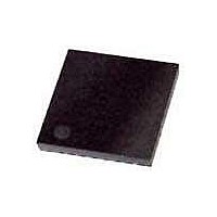
XR18W750IL48-F Exar Corporation, XR18W750IL48-F Datasheet - Page 31

XR18W750IL48-F
Manufacturer Part Number
XR18W750IL48-F
Description
IC WIRELESS UART CTRLR 48QFN
Manufacturer
Exar Corporation
Datasheet
1.XR18W750IL48-F.pdf
(44 pages)
Specifications of XR18W750IL48-F
Package / Case
48-VFQFN Exposed Pad
Function
Controller
Rf Type
General Purpose
Secondary Attributes
I²C Interface
Processor Series
XR18W750
Core
8051
Data Bus Width
8 bit
Data Ram Size
32 KB
Interface Type
I2C, UART
Maximum Clock Frequency
400 KHz
Number Of Timers
1
Operating Supply Voltage
2.25 V to 3.63 V
Maximum Operating Temperature
+ 85 C
Mounting Style
SMD/SMT
3rd Party Development Tools
PK51, CA51, A51, ULINK2
Development Tools By Supplier
XR18W750/753-0A-EB, XR18W750/753-0B-EB
Minimum Operating Temperature
- 40 C
Program Memory Type
EEPROM
Lead Free Status / RoHS Status
Lead free / RoHS Compliant
Lead Free Status / RoHS Status
Lead free / RoHS Compliant, Lead free / RoHS Compliant
Available stocks
Company
Part Number
Manufacturer
Quantity
Price
Company:
Part Number:
XR18W750IL48-F
Manufacturer:
EXAR
Quantity:
120
Part Number:
XR18W750IL48-F
Manufacturer:
EXAR/艾科嘉
Quantity:
20 000
REV. 1.0.0
EMSR[6]: LSR Interrupt Mode
•
•
EMSR[7]: Reserved
For normal operation, this bit should be ’1’.
The FIFO Level Register replaces the Scratchpad Register (during a Read) when FCTR[6] = 1. Note that this is
not identical to the FIFO Data Count Register which can be accessed when LCR = 0xBF.
FLVL[7:0]: FIFO Level Register
This register provides the FIFO counter level for the RX FIFO or the TX FIFO or both depending on EMSR[1:0].
See Table 12
These registers make-up the value of the baud rate divisor.
GENERATOR” ON PAGE 12.
This register contains the device ID (0x0A). Prior to reading this register, DLL and DLM should be set to 0x00.
This register contains the device revision information. For example, 0x01 means revision A. Prior to reading
this register, DLL and DLM should be set to 0x00.
User Programmable Transmit/Receive Trigger Level Register. If both the TX and RX trigger levels are used,
the TX trigger levels must be set before the RX trigger levels.
TRG[7:0]: Trigger Level Register
These bits are used to program desired trigger levels when trigger Table-D is selected. FCTR bit-7 selects
between programming the RX Trigger Level (a logic 0) and the TX Trigger Level (a logic 1).
This register is accessible when LCR = 0xBF. Note that this register is not identical to the FIFO Level Count
Register which is located in the general register set when FCTR bit-6 = 1 (Scratchpad Register Swap). It is
suggested to read the FIFO Level Count Register at the Scratchpad Register location when FCTR bit-6 = 1.
See
FC[7:0]: RX/TX FIFO Level Count
Receive/Transmit FIFO Level Count. Number of characters in Receiver FIFO (FCTR[7] = 0) or Transmitter
FIFO (FCTR[7] = 1) can be read via this register. Reading this register is not recommended when transmitting
or receiving data.
FCTR[1:0]: RTS Hysteresis
User selectable RTS# hysteresis levels for hardware flow control application. After reset, these bits are set to
“0” to select the next trigger level for hardware flow control. See
5.12
5.13
5.14
5.15
5.16
5.17
5.18
Logic 0 = LSR Interrupt Delayed (for 16C550 compatibility, default). LSR bits 2, 3, and 4 will generate an
interrupt when the character with the error is in the RHR.
Logic 1 = LSR Interrupt Immediate. LSR bits 2, 3, and 4 will generate an interrupt as soon as the character is
received into the FIFO.
Table
FIFO Level Register (FLVL) - Read-Only
Baud Rate Generator Registers (DLL and DLM) - Read/Write
Device Identification Register (DVID) - Read Only
Device Revision Register (DREV) - Read Only
Trigger Level Register (TRG) - Write-Only
RX/TX FIFO Level Count Register (FC) - Read-Only
Feature Control Register (FCTR) - Read/Write
12.
for details.
31
Table 13
SEE”PROGRAMMABLE BAUD RATE
for more details.
WIRELESS UART CONTROLLER
XR18W750


