CMF20120D Cree Inc, CMF20120D Datasheet
CMF20120D
Specifications of CMF20120D


Related parts for CMF20120D


CMF20120D Summary of contents
Page 1
... CMF20120D- 1200V 80 mΩ Z-F M OSFET N-Channel Enhancement Mode Silicon Carbide Power MOSFET Subject to change without notice. www.cree.com/power 1 ...
Page 2
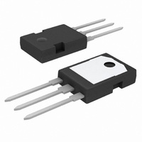
... Repetitive Avalanche Current AR V Gate Source Voltage GS P Power Dissipation tot Operating Junction and Storage Temperature J stg T Solder Temperature L M Mounting Torque d 2 CMF20120D Rev DS(on) I D(MAX) Package TO-247-3 Part Number Package CMF20120D TO-247-3 Value Unit Test Conditions 33 V @20V 25˚C ...
Page 3
... Table of Contents Features.................................................................................................................2 Benefits...........................................................................................................2 Applications.....................................................................................................2 Maximum Ratings...................................................................................................2 Table of Contents....................................................................................................3 Applications Information........................................................................................4 ESD Ratings............................................................................................................7 Electrical Characteristics........................................................................................8 Reverse Diode Characteristics.................................................................................8 Thermal Characteristics..........................................................................................8 Gate Charge Characteristics....................................................................................8 Typical Performance..............................................................................................................9 Clamped Inductive Switch Testing Fixture..............................................................11 Package Dimensions.............................................................................................12 Recommended Solder Pad Layout..........................................................................13 Notice..............................................................................................................14 3 CMF20120D Rev. A ...
Page 4
... The gate resistance should be carefully selected to ensure that the gate drive pulse is adequately dampened. To first order, the gate circuit can be approximated as a simple series RLC circuit driven by a voltage pulse as shown below. 4 CMF20120D Rev than are usually experienced with between - ...
Page 5
... CMF20120D Rev. A ζ ζ ζ ζ LOOP ...
Page 6
... CMF20120D Rev. A Kelvin gate connection with separate source return is highly recommended ...
Page 7
... ESD RATINGS ESD Test ESD-HBM ESD-MM ESD-CDM 7 CMF20120D Rev. A Total Devices Sampled All Devices Passed 1000V All Devices Passed 400V All Devices Passed 1000V Resulting Classification 2 (>2000V) C (>400V) ...
Page 8
... Case to Sink, w/ Thermal Compound θCS R Thermal Resistance From Junction to Ambient θJA Gate Charge Characteristics Symbol Parameter Q Gate to Source Charge gs Q Gate to Drain Charge gd Q Gate Charge Total g 8 CMF20120D Rev. A Min. Typ. Max. Unit 1200 2.5 4 1.8 1 100 10 250 250 80 110 95 130 7.3 6 ...
Page 9
... V (V) GS Figure 3. Typical Transfer Characteristics 1.0E-08 C iss 1.0E-09 C oss 1.0E-10 C rss 1.0E- 100 V (V) DS Fig 5A and 5B. Typical Capacitance vs. Drain – Source Voltage 9 CMF20120D Rev. A 120 100 =10V 25ºC Fig 2. Typical Output Characteristics 1.8 1.6 1.4 1.2 1 0.8 0.6 ° 0.4 0.2 ...
Page 10
... Temp ( C) Fig 7. Inductive Switching Energy(Turn-on) vs Gate Charge (nC) Fig 9. Typical Gate Charge Characteristics @ 25°C 10 CMF20120D Rev. A 1.E-04 1.E-03 1.E-02 Time (s) 600 600 500 500 400 400 V = -2/20V 11.8Ω Total G 300 300 = V 800V 20A D 200 100 100 ...
Page 11
... Fig 11. Switching Waveform Test Circuit 10% Irr 10 Vpk Irr Diode Recovery Waveforms Erec= Diode Reverse Recovery Energy t1 t2 Fig 13. Body Diode Recovery Waveform 11 CMF20120D Rev GS(on) Input ( 10% V GS(off) C2D10120D 10A, 1200V SiC Schottky i D(on) CMF20120D D.U.T. Output ( D(off) trr ∫ Qrr ...
Page 12
... Fig 15. Avalanche Test Circuit Package Dimensions Package TO-247 CMF20120D Rev 1/ Fig 16. Theoretical Avalanche Waveform Inches POS Min Max A .190 .205 A1 .090 .100 A2 .075 .085 b .042 .052 b1 .075 .095 b2 .075 .085 b3 .113 .133 b4 .113 .123 c .022 .027 D .819 .831 D1 .640 .695 D2 .037 ...
Page 13
... Copyright © 2010-2011 Cree, Inc. All rights reserved. The information in this document is subject to change without notice. Cree and the Cree logo are registered trademarks and Z-REC and Z-FET are trademarks of Cree, Inc CMF20120D Rev. A TO-247-3 Part Number Package CMF20120D TO-247-3 Cree, Inc ...