CMF20120D Cree Inc, CMF20120D Datasheet - Page 6
CMF20120D
Manufacturer Part Number
CMF20120D
Description
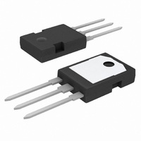
SIC MOSFET N-CH 1200V TO-247-3
Manufacturer
Cree Inc
Series
SiC MOSFETr
Specifications of CMF20120D
Mfg Application Notes
SiC MOSFETs Application Considerations
Fet Type
SiCFET N-Channel, Silicon Carbide
Fet Feature
Standard
Rds On (max) @ Id, Vgs
110 mOhm @ 20A, 20V
Drain To Source Voltage (vdss)
1200V (1.2kV)
Current - Continuous Drain (id) @ 25° C
33A
Vgs(th) (max) @ Id
4V @ 1mA
Gate Charge (qg) @ Vgs
90.8nC @ 20V
Input Capacitance (ciss) @ Vds
1915pF @ 800V
Power - Max
150W
Mounting Type
Through Hole
Package / Case
TO-247-3
Transistor Polarity
N Channel
Continuous Drain Current Id
33A
Drain Source Voltage Vds
1200V
On Resistance Rds(on)
0.08ohm
Rds(on) Test Voltage Vgs
20V
Configuration
Single
Resistance Drain-source Rds (on)
80 mOhms
Forward Transconductance Gfs (max / Min)
7.3 S, 6.8 S
Drain-source Breakdown Voltage
1200 V
Gate-source Breakdown Voltage
25 V
Continuous Drain Current
33 A
Power Dissipation
150 W
Mounting Style
Through Hole
Gate Charge Qg
90.8 nC
Lead Free Status / RoHS Status
Lead free / RoHS Compliant
Lead Free Status / RoHS Status
Lead free / RoHS Compliant


6
A schematic of the gate driver circuit used for characterization of the SiC MOSFET
is shown below:
The gate driver is an IXYS IXDI414. This device has a 35 V ouput swing, output
resistance of 0.6 Ω typical, and a peak current capability of 14 A. The external
gate resistance used for characterization of the SiC MOSFET was 6.8 Ω. Careful
consideration needs to be given to the selection of the gate driver. The typical
application error is selection of a gate driver that has adequate swing, but output
+VCC
GND
-VEE
PULSE GEN INPUT
J1
BNC
Stray inductance on source lead causes load
di/dt to be fed back into gate drive which
causes the following:
•
•
CMF20120D Rev. A
1
DRIVE
Switch di/dt is limited
Could cause oscillation
R5
120
10u
10u
C3
C6
+VCC
-VEE
R6
120
R4
330
20V
2
3
+VCC
ISO1
6N137
R GATE
C10
100n
L STRAY
1
U1
IN
LM2931T-5.0
-VEE
-VEE
OUT
THESE COMPONENTS ARE
LOCATED ON THE -VEE
PLANE
3
SiC DMOS
LOAD CURRENT
LOAD CURRENT
C11
100u
6.3V
8
7
6
C14
100n
+VCC
R2
390
R1
1
-VEE
1
2
3
4
U2
VCC
IN
NC
GND
IXDI414
C7
10u
C9
100n
C13
10n
VCC
GND
OUT
OUT
8
7
6
5
-VEE
Kelvin gate connection with separate
source return is highly recommended
-VEE
-VEE
-VEE
-VEE
-VEE
-VEE
-VEE
-VEE
-VEE
-VEE
-VEE
-VEE
DRIVE
C1
10u
C2
100n
C4
100n
C5
100n
C8
100n
C12
100n
C15
100n
C16
100n
C17
100n
C18
100n
C19
100n
C20
10u
R3
TBD 1206
R7
TBD 1206
R8
TBD 1206
20V
THESE COMPONENTS ARE
LOCATED ON THE GND
PLANE
VGS MONITOR
D1
RB160M-60
D2
RB160M-60
R GATE
J2
BNC
1
SiC DMOS
L STRAY
PIN 1 SOURCE
PIN 2 GATE
Related parts for CMF20120D
Image
Part Number
Description
Manufacturer
Datasheet
Request
R

Part Number:
Description:
CREE PLCC4 SMD LED WHITE
Manufacturer:
Cree Inc
Datasheet:
Part Number:
Description:
CREE PLCC4 SMD LED WHITE
Manufacturer:
Cree Inc
Datasheet:

Part Number:
Description:
CREE PLCC4 SMD LED WHITE
Manufacturer:
Cree Inc
Datasheet:
Part Number:
Description:
CREE PLCC4 SMD LED WHITE
Manufacturer:
Cree Inc
Datasheet:
Part Number:
Description:
CREE PLCC4 SMD LED WHITE
Manufacturer:
Cree Inc
Datasheet:

Part Number:
Description:
DIODE SCHOTTKY 600V 16.5A TO-247
Manufacturer:
Cree Inc
Datasheet:

Part Number:
Description:
DIODE SCHOTTKY 600V 6A TO220-2
Manufacturer:
Cree Inc
Datasheet:
Part Number:
Description:
DIODE SCHOTTKY 600V 10A TO220-2
Manufacturer:
Cree Inc
Datasheet:

Part Number:
Description:
IC AMP MMIC HEMT 25W 780019PKG
Manufacturer:
Cree Inc
Datasheet:

Part Number:
Description:
Cree� XLamp� XT-E LEDs
Manufacturer:
CREE [Cree, Inc]
Datasheet:
Part Number:
Description:
Cree� EZBright290� LEDs
Manufacturer:
CREE [Cree, Inc]
Datasheet:

Part Number:
Description:
DIODE SCHOT 600V 2A ZREC TO220
Manufacturer:
Cree Inc
Datasheet:
Part Number:
Description:
DIODE SCHOT 600V 3A ZREC TO252
Manufacturer:
Cree Inc
Datasheet: