CMF20120D Cree Inc, CMF20120D Datasheet - Page 5
CMF20120D
Manufacturer Part Number
CMF20120D
Description
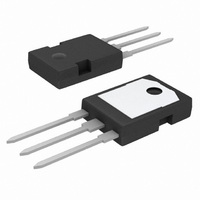
SIC MOSFET N-CH 1200V TO-247-3
Manufacturer
Cree Inc
Series
SiC MOSFETr
Specifications of CMF20120D
Mfg Application Notes
SiC MOSFETs Application Considerations
Fet Type
SiCFET N-Channel, Silicon Carbide
Fet Feature
Standard
Rds On (max) @ Id, Vgs
110 mOhm @ 20A, 20V
Drain To Source Voltage (vdss)
1200V (1.2kV)
Current - Continuous Drain (id) @ 25° C
33A
Vgs(th) (max) @ Id
4V @ 1mA
Gate Charge (qg) @ Vgs
90.8nC @ 20V
Input Capacitance (ciss) @ Vds
1915pF @ 800V
Power - Max
150W
Mounting Type
Through Hole
Package / Case
TO-247-3
Transistor Polarity
N Channel
Continuous Drain Current Id
33A
Drain Source Voltage Vds
1200V
On Resistance Rds(on)
0.08ohm
Rds(on) Test Voltage Vgs
20V
Configuration
Single
Resistance Drain-source Rds (on)
80 mOhms
Forward Transconductance Gfs (max / Min)
7.3 S, 6.8 S
Drain-source Breakdown Voltage
1200 V
Gate-source Breakdown Voltage
25 V
Continuous Drain Current
33 A
Power Dissipation
150 W
Mounting Style
Through Hole
Gate Charge Qg
90.8 nC
Lead Free Status / RoHS Status
Lead free / RoHS Compliant
Lead Free Status / RoHS Status
Lead free / RoHS Compliant


5
As shown, minimizing L
dampening. Minimizing L
strongly recommended that the gate drive be located as close to the SiC MOSFET
as possible to minimize L
An external resistance of 6.8 Ω was used to characterize this device.
Lower values of external gate resistance can be used so long as the gate fidelity is
maintained. In the event that no external gate resistance is used, it is suggested
that the gate current be checked to indirectly verify that there is no ringing present
in the gate circuit. This can be accomplished with a very small current transformer.
A recommended setup is a two-stage current transformer as shown below:
V
CMF20120D Rev. A
PULSE
GATE DRIVE INPUT
R
LOOP
LOOP
LOOP
LOOP
L
LOOP
minimizes the value of R
. The internal gate resistance of the SiC MOSFET is 5 Ω.
also minimizes the rise/fall time. Therefore, it is
VCC
VEE
+
-
GATE DRIVER
C
GATE
IG SENSE
T1
∴
ζ ζ ζ ζ
=
LOOP
R
R
LOOP
needed for critical
LOOP
2
≥
C
L
SiC DMOSFET
LOOP
2
GATE
C
L
≥
LOOP
GATE
1
Related parts for CMF20120D
Image
Part Number
Description
Manufacturer
Datasheet
Request
R

Part Number:
Description:
CREE PLCC4 SMD LED WHITE
Manufacturer:
Cree Inc
Datasheet:
Part Number:
Description:
CREE PLCC4 SMD LED WHITE
Manufacturer:
Cree Inc
Datasheet:

Part Number:
Description:
CREE PLCC4 SMD LED WHITE
Manufacturer:
Cree Inc
Datasheet:
Part Number:
Description:
CREE PLCC4 SMD LED WHITE
Manufacturer:
Cree Inc
Datasheet:
Part Number:
Description:
CREE PLCC4 SMD LED WHITE
Manufacturer:
Cree Inc
Datasheet:

Part Number:
Description:
DIODE SCHOTTKY 600V 16.5A TO-247
Manufacturer:
Cree Inc
Datasheet:

Part Number:
Description:
DIODE SCHOTTKY 600V 6A TO220-2
Manufacturer:
Cree Inc
Datasheet:
Part Number:
Description:
DIODE SCHOTTKY 600V 10A TO220-2
Manufacturer:
Cree Inc
Datasheet:

Part Number:
Description:
IC AMP MMIC HEMT 25W 780019PKG
Manufacturer:
Cree Inc
Datasheet:

Part Number:
Description:
Cree� XLamp� XT-E LEDs
Manufacturer:
CREE [Cree, Inc]
Datasheet:
Part Number:
Description:
Cree� EZBright290� LEDs
Manufacturer:
CREE [Cree, Inc]
Datasheet:

Part Number:
Description:
DIODE SCHOT 600V 2A ZREC TO220
Manufacturer:
Cree Inc
Datasheet:
Part Number:
Description:
DIODE SCHOT 600V 3A ZREC TO252
Manufacturer:
Cree Inc
Datasheet: