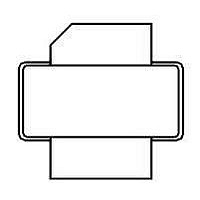
BLF7G22LS-200,112 NXP Semiconductors, BLF7G22LS-200,112 Datasheet - Page 3

BLF7G22LS-200,112
Manufacturer Part Number
BLF7G22LS-200,112
Description
TRANSISTOR PWR LDMOS SOT502
Manufacturer
NXP Semiconductors
Specifications of BLF7G22LS-200,112
Package / Case
SOT502B
Transistor Type
LDMOS
Frequency
2.11GHz ~ 2.17GHz
Gain
18.5dB
Voltage - Rated
65V
Current Rating
29.5A
Current - Test
1.62A
Voltage - Test
28V
Power - Output
30W
Mounting Style
SMD/SMT
Configuration
Single
Drain-source Breakdown Voltage
65 V
Continuous Drain Current
29.5 A
Channel Type
N
Channel Mode
Enhancement
Drain Source Voltage (max)
65V
Output Power (max)
30W(Typ)
Power Gain (typ)@vds
18.5@28VdB
Frequency (min)
2.11GHz
Frequency (max)
2.17GHz
Package Type
LDMOST
Pin Count
3
Forward Transconductance (typ)
18.9S
Drain Source Resistance (max)
54(Typ)@6.05Vmohm
Operating Temp Range
-65C to 200C
Drain Efficiency (typ)
31%
Mounting
Surface Mount
Mode Of Operation
2-Carrier W-CDMA
Number Of Elements
1
Vswr (max)
10
Screening Level
Military
Lead Free Status / RoHS Status
Lead free / RoHS Compliant
Noise Figure
-
Lead Free Status / Rohs Status
Compliant
NXP Semiconductors
6. Characteristics
7. Test information
BLF7G22L-200_7G22LS-200
Preliminary data sheet
7.1 Ruggedness in class-AB operation
Table 6.
T
Table 7.
Mode of operation: 2-carrier W-CDMA; PAR = 8.4 dB at 0.01 % probability on the CCDF; 3GPP test
model 1; 1-64 DPCH; f
RF performance at V
class-AB production test circuit.
The BLF7G22L-200 and BLF7G22LS-200 are capable of withstanding a load mismatch
corresponding to VSWR = 10 : 1 through all phases under the following conditions:
V
Symbol Parameter
V
V
I
I
I
g
R
Symbol
P
G
RL
ACPR
η
DSS
DSX
GSS
j
DS
fs
D
(BR)DSS
GS(th)
L(AV)
DS(on)
p
= 25
in
= 28 V; I
°
C unless otherwise specified.
drain-source breakdown voltage V
gate-source threshold voltage
drain leakage current
drain cut-off current
gate leakage current
forward transconductance
drain-source on-state resistance V
Characteristics
Functional test information
Parameter
average output power
power gain
input return loss
drain efficiency
adjacent channel power ratio
Dq
= 1620 mA; P
All information provided in this document is subject to legal disclaimers.
DS
BLF7G22L-200; BLF7G22LS-200
1
= 28 V; I
= 2112.5 MHz; f
Rev. 3 — 1 April 2011
Dq
L
= 200 W (CW); f = 2110 MHz to 2170 MHz.
= 1620 mA; T
2
= 2117.5 MHz; f
Conditions
V
V
V
V
V
V
I
D
GS
DS
GS
GS
DS
GS
DS
GS
= 5.25 A
case
= 10 V; I
= 10 V
= 10 V; I
= 0 V; I
= 0 V; V
= V
= 11 V; V
= V
Conditions
P
P
P
P
L(AV)
L(AV)
L(AV)
L(AV)
GS(th)
GS(th)
= 25
= 55 W
= 55 W
= 55 W
= 55 W
D
DS
D
D
3
= 1.5 mA
+ 3.75 V;
DS
+ 3.75 V;
°
= 150 mA
C; unless otherwise specified; in a
= 5.25 A
= 2162.5 MHz; f
= 28 V
= 0 V
Min
-
16.8 18.5
-
27
-
Power LDMOS transistor
Min
65
1.5
-
42
-
-
-
4
Typ
55
−15
31
−31
= 2167.5 MHz;
© NXP B.V. 2011. All rights reserved.
Typ
-
1.9
-
50.8
-
18.9
0.054 -
Max
-
-
−6
-
−25.5 dBc
Max
-
2.3
4.2
-
420
-
W
Unit
dB
dB
%
3 of 13
Unit
V
V
μA
A
nA
S
Ω


