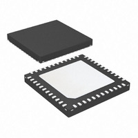
DS99R124QSQ/NOPB National Semiconductor, DS99R124QSQ/NOPB Datasheet - Page 18

DS99R124QSQ/NOPB
Manufacturer Part Number
DS99R124QSQ/NOPB
Description
IC DESERIALIZER 18BIT 48LLP
Manufacturer
National Semiconductor
Datasheet
1.DS99R124QSQXNOPB.pdf
(24 pages)
Specifications of DS99R124QSQ/NOPB
Function
Deserializer
Data Rate
1.2Gbps
Input Type
Serial
Output Type
LVDS
Number Of Inputs
1
Number Of Outputs
4
Voltage - Supply
1.71 V ~ 1.89 V, 3 V ~ 3.6 V
Operating Temperature
-40°C ~ 105°C
Mounting Type
Surface Mount
Package / Case
48-WFQFN, Exposed Pad
Lead Free Status / RoHS Status
Lead free / RoHS Compliant
Other names
DS99R124QSQ
Available stocks
Company
Part Number
Manufacturer
Quantity
Price
Company:
Part Number:
DS99R124QSQ/NOPB
Manufacturer:
AVAGO
Quantity:
65
www.national.com
Serial Bus Control — Optional
The DS99R124 may also be configured by the use of a serial
control bus that is I2C protocol compatible. By default, the I2C
reg_0x00'h is set to 00'h and all configuration is set by control/
strap pins. A write of 01'h to reg_0x00'h will enable/allow con-
figuration by registers; this will override the control/strap pins.
Multiple devices may share the serial control bus since mul-
tiple addresses are supported. See
The serial bus is comprised of three pins. The SCL is a Serial
Bus Clock Input. The SDA is the Serial Bus Data Input / Out-
put signal. Both SCL and SDA signals require an external pull
up resistor to V
sistor to V
adjusted for capacitive loading and data rate requirements.
The signals are either pulled High, or driven Low.
The third pin is the ID[X] pin. This pin sets one of four possible
device addresses. Two different connections are possible.
The pin may be pulled to V
kΩ resistor. Or a 10 kΩ pull up resistor (to V
V
to set other three possible addresses may be used. See
5
The Serial Bus protocol is controlled by START, START-Re-
peated, and STOP phases. A START occurs when SCL
transitions Low while SDA is High. A STOP occurs when SDA
transition High while SCL is also HIGH. See
DDIO
for the Des.
)) and a pull down resistor of the recommended value
FIGURE 19. Serial Control Bus Connection
DDIO
DDIO
may be used. The resistor value may be
. For most applications a 4.7 k pull up re-
DD
(1.8V, NOT V
Figure
FIGURE 22. Serial Control Bus — WRITE
19.
FIGURE 21. Serial Control Bus — READ
Figure 20
DDIO
DD
)) with a 10
1.8V, NOT
30105241
Table
18
To communicate with a remote device, the host controller
(master) sends the slave address and listens for a response
from the slave. This response is referred to as an acknowl-
edge bit (ACK). If a slave on the bus is addressed correctly,
it Acknowledges (ACKs) the master by driving the SDA bus
low. If the address doesn't match a device's slave address, it
Not-acknowledges (NACKs) the master by letting SDA be
pulled High. ACKs also occur on the bus when data is being
transmitted. When the master is writing data, the slave ACKs
after every data byte is successfully received. When the mas-
ter is reading data, the master ACKs after every data byte is
received to let the slave know it wants to receive another data
byte. When the master wants to stop reading, it NACKs after
the last data byte and creates a stop condition on the bus. All
communication on the bus begins with either a Start condition
or a Repeated Start condition. All communication on the bus
ends with a Stop condition. A READ is shown in
and a WRITE is shown in
If the Serial Bus is not required, the three pins may be left
open (NC).
Resistor
RID kΩ
(5%tol)
Open
0.47
TABLE 5. ID[x] Resistor Value – DS99R124Q Des
2.7
8.2
FIGURE 20. START and STOP Conditions
7b' 111 0001 (h'71)
7b' 111 0010 (h'72)
7b' 111 0011 (h'73)
7b' 111 0110 (h'76)
Address
7'b
Figure
30105239
22.
8b' 1110 1100 (h'EC)
8b' 1110 0010 (h'E2)
8b' 1110 0100 (h'E4)
8b' 1110 0110 (h'E6)
30105238
0 appended
Address
(WRITE)
8'b
Figure 21
30105251


