DS99R124QSQ/NOPB National Semiconductor, DS99R124QSQ/NOPB Datasheet - Page 5
DS99R124QSQ/NOPB
Manufacturer Part Number
DS99R124QSQ/NOPB
Description
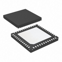
IC DESERIALIZER 18BIT 48LLP
Manufacturer
National Semiconductor
Datasheet
1.DS99R124QSQXNOPB.pdf
(24 pages)
Specifications of DS99R124QSQ/NOPB
Function
Deserializer
Data Rate
1.2Gbps
Input Type
Serial
Output Type
LVDS
Number Of Inputs
1
Number Of Outputs
4
Voltage - Supply
1.71 V ~ 1.89 V, 3 V ~ 3.6 V
Operating Temperature
-40°C ~ 105°C
Mounting Type
Surface Mount
Package / Case
48-WFQFN, Exposed Pad
Lead Free Status / RoHS Status
Lead free / RoHS Compliant
Other names
DS99R124QSQ
Available stocks
Company
Part Number
Manufacturer
Quantity
Price
Company:

Part Number:
DS99R124QSQ/NOPB
Manufacturer:
AVAGO
Quantity:
65


FPD-Link LVDS Output
|V
V
ΔV
V
ΔV
I
I
3.3 V I/O LVCMOS DC SPECIFICATIONS – V
V
V
I
Symbol
OS
OZ
IN
ODp-p
OS
IH
IL
OD
Absolute Maximum Ratings
If Military/Aerospace specified devices are required,
please contact the National Semiconductor Sales Office/
Distributors for availability and specifications.
DC Electrical Characteristics
Over recommended operating supply and temperature ranges unless otherwise specified.
Supply Voltage – V
Supply Voltage – V
Supply Voltage – V
LVCMOS I/O Voltage
Receiver Input Voltage
LVDS Output Voltage
Junction Temperature
Storage Temperature
Lead Temperature
(Soldering, 4s)
48L LLP Package
Maximum Power Dissipation
Capacity at 25°C
θ
θ
ESD Rating (IEC, powered-up only), R
OD
OS
|
Derate above 25°C
Air Discharge
(R
Contact Discharge
(R
JA
JC
IN+
IN+
, R
, R
Differential Output Voltage
Differential Output Voltage
A-B
Output Voltage Unbalance
Offset Voltage
Offset Voltage Unbalance
Output Short Circuit Current
Output TRI-STATE® Current
High Level Input Voltage
Low Level Input Voltage
Input Current
IN−
IN−
)
)
Parameter
DDn
DDTX
DDIO
(1.8V)
(3.3V)
−0.3V to +(VDDIO + 0.3V)
−0.3V to (VDDTX + 0.3V)
−0.3V to (VDD + 0.3V)
D
= 330Ω, C
R
Vout = GND
OEN = GND,
Vout =V
V
IN
L
−65°C to +150°C
= 100Ω
= 0V or V
DDIO
−0.3V to +2.5V
−0.3V to +4.0V
−0.3V to +4.0V
(Note
DDTX
1/ θ
= 3.0 to 3.6V
27.7 °C/W
S
3.0 °C/W
≥
= 150pF
+150°C
+260°C
≥
, or GND
JA
±30 kV
Conditions
DDIO
1)
±6 kV
°C/W
5
VODSEL = L
VODSEL = H
VODSEL = L
VODSEL = H
VODSEL = L
VODSEL = H
Supply Voltage (V
LVCMOS Supply
Voltage (V
LVCMOS Supply
Voltage (V
Operating Free Air
TxCLK Clock Frequency
Supply Noise
Recommended Operating
Conditions
ESD Rating (ISO10605), R
ESD Rating (ISO10605), R
ESD Rating (HBM)
ESD Rating (CDM)
ESD Rating (MM)
Air Discharge
(R
Contact Discharge
(R
Air Discharge
(R
Contact Discharge
(R
Temperature (T
IN+
IN+
IN+
IN+
, R
, R
, R
, R
DDIO
DDIO
IN−
IN−
IN−
IN−
TxCLKOUT+,
TxCLKOUT-,
TxOUT[2:0]+,
TxOUT[2:0]-
PDB,
VODSEL,
OEN,
OSS_SEL,
LFMODE,
SSC[2:0],
BISTEN,
BISTM
(Note
Pin/Freq.
)
)
)
)
)
)
DDn
7)
A
)
)
(Note
1.71
1.71
Min
−40
3.0
D
D
5
GND
2,
Min
100
200
−15
1.0
-10
2.2
= 330Ω, C
= 2kΩ, C
Note
Nom
+25
1.8
1.8
3.3
3) and
S
Typ
250
400
500
800
1.2
1.2
±1
-5
S
1
1
= 150 & 330pF
= 150 & 330pF
(Note
+105
Max
1.89
1.89
100
3.6
43
V
Max
+10
+15
400
600
1.5
0.8
www.national.com
50
50
DDIO
≥
4)
±1.25 kV
≥
≥
≥
≥
≥
≥
±15 kV
±15 kV
±250 V
±8 kV
±8 kV
±8 kV
mV
Units
MHz
mVp-p
mVp-p
°C
Units
V
V
V
mV
mV
mV
mV
mA
µA
μA
P-P
V
V
V
V
Related parts for DS99R124QSQ/NOPB
Image
Part Number
Description
Manufacturer
Datasheet
Request
R

Part Number:
Description:
EVAL BOARD FOR DS99R124Q
Manufacturer:
National Semiconductor
Datasheet:
Part Number:
Description:
National Semiconductor [8-Bit D/A Converter]
Manufacturer:
National Semiconductor
Datasheet:
Part Number:
Description:
National Semiconductor [Media Coprocessor]
Manufacturer:
National Semiconductor
Datasheet:
Part Number:
Description:
Digitally Controlled Tone and Volume Circuit with Stereo Audio Power Amplifier, Microphone Preamp Stage and National 3D Sound
Manufacturer:
National Semiconductor
Datasheet:
Part Number:
Description:
Digitally Controlled Tone and Volume Circuit with Stereo Audio Power Amplifier, Microphone Preamp Stage and National 3D Sound
Manufacturer:
National Semiconductor
Datasheet:
Part Number:
Description:
AC97 Rev 2 Codec with Sample Rate Conversion and National 3D Sound
Manufacturer:
National Semiconductor
Part Number:
Description:
Manufacturer:
National Semiconductor
Datasheet:
Part Number:
Description:
Manufacturer:
National Semiconductor
Datasheet:
Part Number:
Description:
General Purpose, Low Voltage, Low Power, Rail-to-Rail Output Operational Amplifiers
Manufacturer:
National Semiconductor
Datasheet:
Part Number:
Description:
8-bit 20 MSPS flash A/D converter.
Manufacturer:
National Semiconductor
Datasheet:
Part Number:
Description:
Low Noise Quad Operational Amplifier
Manufacturer:
National Semiconductor
Datasheet:
Part Number:
Description:
Quad Differential Line Receivers
Manufacturer:
National Semiconductor
Datasheet:
Part Number:
Description:
Quad High Speed Trapezoidal? Bus Transceiver
Manufacturer:
National Semiconductor
Datasheet:
Part Number:
Description:
Dual Line Receiver
Manufacturer:
National Semiconductor
Datasheet: