DS99R124QSQ/NOPB National Semiconductor, DS99R124QSQ/NOPB Datasheet - Page 3
DS99R124QSQ/NOPB
Manufacturer Part Number
DS99R124QSQ/NOPB
Description
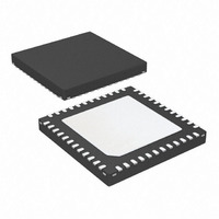
IC DESERIALIZER 18BIT 48LLP
Manufacturer
National Semiconductor
Datasheet
1.DS99R124QSQXNOPB.pdf
(24 pages)
Specifications of DS99R124QSQ/NOPB
Function
Deserializer
Data Rate
1.2Gbps
Input Type
Serial
Output Type
LVDS
Number Of Inputs
1
Number Of Outputs
4
Voltage - Supply
1.71 V ~ 1.89 V, 3 V ~ 3.6 V
Operating Temperature
-40°C ~ 105°C
Mounting Type
Surface Mount
Package / Case
48-WFQFN, Exposed Pad
Lead Free Status / RoHS Status
Lead free / RoHS Compliant
Other names
DS99R124QSQ
Available stocks
Company
Part Number
Manufacturer
Quantity
Price
Company:

Part Number:
DS99R124QSQ/NOPB
Manufacturer:
AVAGO
Quantity:
65


Pin Name
LVCMOS Outputs
OS[2:0]
LOCK
Control and Configuration
PDB
VODSEL
OEN
OSS_SEL
LFMODE
SSC[2:0]
RES[1:0]
Control and Configuration — STRAP PIN
For a High State, use a 10 kΩ pull up to VDDIO; for a Low State, the IO includes an internal pull down. The STRAP pin is read upon
power-up and set device configuration. Pin number listed along with shared LVCMOS Output name in square bracket.
EQ
Optional BIST Mode
BISTEN
BISTM
PASS
Optional Serial Bus Control Interface
SCL
SDA
Pin #
10, 11, 12
27
1
33
34
35
36
7, 2, 3
37, 15
28 [PASS]
29
30
28
5
4
I/O, Type
O, LVMOS
O, LVMOS
I, LVCMOS
w/ pull-down
I, LVCMOS
w/ pull-down
I, LVCMOS
w/ pull-down
I, LVCMOS
w/ pull-down
I, LVCMOS
w/ pull-down
I, LVCMOS
w/ pull-down
I, LVCMOS
w/ pull-down
STRAP
I, LVCMOS
w/ pull-down
I, LVCMOS
w/ pull-down
I, LVCMOS
w/ pull-down
O, LVCMOS PASS Output (BIST Mode) – Optional
I, LVCMOS
I/O,
LVCMOS
Open Drain
Description
Over-Sampled Low Frequency Outputs
These bits map to the DS99R421's OS[2:0] over-sampled low-frequency inputs. Signals
must be slower the TxCLK/5. On the DS90UR241 these map to the DIN[23:21] inputs. OS0
= DIN21, OS1 = DIN22, OS2 = DIN23.
LOCK Status Output
LOCK = 1, PLL is locked, outputs are active.
LOCK = 0, PLL is unlocked, output states determined by OSS_SEL.
Maybe used as a Link Status or to flag when the Video Data is active (ON/OFF).
Power Down Mode Input
PDB = 1, Device is enabled (normal operation)
PDB = 0, Device is in power-down, the output are controlled by the settings. Control registers
are RESET.
Differential Driver Output Voltage Select
VODSEL = 1, LVDS VOD is ±400 mV, 800 mVp-p (typ) — Long Cable / De-E Applications
VODSEL = 0, LVDS VOD is ±250 mV, 500 mVp-p (typ)
SeeTable 2
Output Enable Input
OEN = 1, FPD-Link outputs are enabled (active).
OEN = 0, FPD-Link outputs are TRI-STATE.
Output Sleep State Select Input
See
Low Frequency Mode — Pin or Register Control
LF_MODE = 1, low frequency mode (TxCLKOUT = 5-20 MHz)
LF_MODE = 0, high frequency mode (TxCLKOUT = 20-43 MHz)
Spread Spectrum Clock Generation (SSCG) Range Select
SeeTable 3
Reserved
Tie Low
EQ Gain Control of FPD-Link II Input
EQ = 1, EQ gain is enabled (~13 dB)
EQ = 0, EQ gain is disabled (~1.625 dB)
BIST Enable Input – Optional
BISTEN = 1, BIST Mode is enabled.
BISTEN = 0, normal mode.
BIST Mode Input – Optional
BISTM = 1, selects Payload Error Mode
BISTM = 0, selects Pass / Fail Result-Only Mode
PASS = 1, no errors detected
PASS = 0, errors detected
Leave open if unused. Route to a test point (pad) recommended.
Serial Control Bus Clock Input - Optional
SCL requires an external pull-up resistor to V
Serial Control Bus Data Input / Output - Optional
SDA requires an external pull-up resistor to V
Table 1
and
Table 4
3
DDIO
DDIO
.
.
www.national.com
Related parts for DS99R124QSQ/NOPB
Image
Part Number
Description
Manufacturer
Datasheet
Request
R

Part Number:
Description:
EVAL BOARD FOR DS99R124Q
Manufacturer:
National Semiconductor
Datasheet:
Part Number:
Description:
National Semiconductor [8-Bit D/A Converter]
Manufacturer:
National Semiconductor
Datasheet:
Part Number:
Description:
National Semiconductor [Media Coprocessor]
Manufacturer:
National Semiconductor
Datasheet:
Part Number:
Description:
Digitally Controlled Tone and Volume Circuit with Stereo Audio Power Amplifier, Microphone Preamp Stage and National 3D Sound
Manufacturer:
National Semiconductor
Datasheet:
Part Number:
Description:
Digitally Controlled Tone and Volume Circuit with Stereo Audio Power Amplifier, Microphone Preamp Stage and National 3D Sound
Manufacturer:
National Semiconductor
Datasheet:
Part Number:
Description:
AC97 Rev 2 Codec with Sample Rate Conversion and National 3D Sound
Manufacturer:
National Semiconductor
Part Number:
Description:
Manufacturer:
National Semiconductor
Datasheet:
Part Number:
Description:
Manufacturer:
National Semiconductor
Datasheet:
Part Number:
Description:
General Purpose, Low Voltage, Low Power, Rail-to-Rail Output Operational Amplifiers
Manufacturer:
National Semiconductor
Datasheet:
Part Number:
Description:
8-bit 20 MSPS flash A/D converter.
Manufacturer:
National Semiconductor
Datasheet:
Part Number:
Description:
Low Noise Quad Operational Amplifier
Manufacturer:
National Semiconductor
Datasheet:
Part Number:
Description:
Quad Differential Line Receivers
Manufacturer:
National Semiconductor
Datasheet:
Part Number:
Description:
Quad High Speed Trapezoidal? Bus Transceiver
Manufacturer:
National Semiconductor
Datasheet:
Part Number:
Description:
Dual Line Receiver
Manufacturer:
National Semiconductor
Datasheet: