DS99R124QSQ/NOPB National Semiconductor, DS99R124QSQ/NOPB Datasheet - Page 9
DS99R124QSQ/NOPB
Manufacturer Part Number
DS99R124QSQ/NOPB
Description
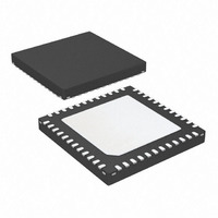
IC DESERIALIZER 18BIT 48LLP
Manufacturer
National Semiconductor
Datasheet
1.DS99R124QSQXNOPB.pdf
(24 pages)
Specifications of DS99R124QSQ/NOPB
Function
Deserializer
Data Rate
1.2Gbps
Input Type
Serial
Output Type
LVDS
Number Of Inputs
1
Number Of Outputs
4
Voltage - Supply
1.71 V ~ 1.89 V, 3 V ~ 3.6 V
Operating Temperature
-40°C ~ 105°C
Mounting Type
Surface Mount
Package / Case
48-WFQFN, Exposed Pad
Lead Free Status / RoHS Status
Lead free / RoHS Compliant
Other names
DS99R124QSQ
Available stocks
Company
Part Number
Manufacturer
Quantity
Price
Company:

Part Number:
DS99R124QSQ/NOPB
Manufacturer:
AVAGO
Quantity:
65


Note 1: “Absolute Maximum Ratings” indicate limits beyond which damage to the device may occur, including inoperability and degradation of device reliability
and/or performance. Functional operation of the device and/or non-degradation at the Absolute Maximum Ratings or other conditions beyond those indicated in
the Recommended Operating Conditions is not implied. The Recommended Operating Conditions indicate conditions at which the device is functional and the
device should not be operated beyond such conditions.
Note 2: The Electrical Characteristics tables list guaranteed specifications under the listed Recommended Operating Conditions except as otherwise modified
or specified by the Electrical Characteristics Conditions and/or Notes. Typical specifications are estimations only and are not guaranteed.
Note 3: Typical values represent most likely parametric norms at V
Operation Conditions at the time of product characterization and are not guaranteed.
Note 4: Current into device pins is defined as positive. Current out of a device pin is defined as negative. Voltages are referenced to ground except VOD, ΔVOD,
VTH and VTL which are differential voltages.
Note 5: t
Note 6: t
Note 7: Supply noise testing was done with minimum capacitors on the PCB. A sinusoidal signal is AC coupled to the V
mVp-p measured at the device V
frequency on the Ser is less than 750 kHz. The Des on the other hand shows no error when the noise frequency is less than 400 kHz.
Note 8: Specification is guaranteed by characterization and is not tested in production.
Note 9: Specification is guaranteed by design and is not tested in production.
AC Timing Diagrams and Test Circuits
DDLT
DCCJ
is the time required by the deserializer to obtain lock when exiting power-down state with an active PCLK.
is the maximum amount of jitter between adjacent clock cycles.
DDn
pins. Bit error rate testing of input to the Ser and output of the Des with 10 meter cable shows no error when the noise
FIGURE 1. Checkerboard Data Pattern
FIGURE 2. LVCMOS Transition Times
DDn
= 1.8V, V
9
DDTX
= 3.3V, V
DDIO
= 1.8V or 3.3V, Ta = +25 °C, and at the Recommended
DDn
30105205
(1.8V) supply with amplitude = 100
30105232
www.national.com
Related parts for DS99R124QSQ/NOPB
Image
Part Number
Description
Manufacturer
Datasheet
Request
R

Part Number:
Description:
EVAL BOARD FOR DS99R124Q
Manufacturer:
National Semiconductor
Datasheet:
Part Number:
Description:
National Semiconductor [8-Bit D/A Converter]
Manufacturer:
National Semiconductor
Datasheet:
Part Number:
Description:
National Semiconductor [Media Coprocessor]
Manufacturer:
National Semiconductor
Datasheet:
Part Number:
Description:
Digitally Controlled Tone and Volume Circuit with Stereo Audio Power Amplifier, Microphone Preamp Stage and National 3D Sound
Manufacturer:
National Semiconductor
Datasheet:
Part Number:
Description:
Digitally Controlled Tone and Volume Circuit with Stereo Audio Power Amplifier, Microphone Preamp Stage and National 3D Sound
Manufacturer:
National Semiconductor
Datasheet:
Part Number:
Description:
AC97 Rev 2 Codec with Sample Rate Conversion and National 3D Sound
Manufacturer:
National Semiconductor
Part Number:
Description:
Manufacturer:
National Semiconductor
Datasheet:
Part Number:
Description:
Manufacturer:
National Semiconductor
Datasheet:
Part Number:
Description:
General Purpose, Low Voltage, Low Power, Rail-to-Rail Output Operational Amplifiers
Manufacturer:
National Semiconductor
Datasheet:
Part Number:
Description:
8-bit 20 MSPS flash A/D converter.
Manufacturer:
National Semiconductor
Datasheet:
Part Number:
Description:
Low Noise Quad Operational Amplifier
Manufacturer:
National Semiconductor
Datasheet:
Part Number:
Description:
Quad Differential Line Receivers
Manufacturer:
National Semiconductor
Datasheet:
Part Number:
Description:
Quad High Speed Trapezoidal? Bus Transceiver
Manufacturer:
National Semiconductor
Datasheet:
Part Number:
Description:
Dual Line Receiver
Manufacturer:
National Semiconductor
Datasheet: