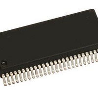
KIT33937AEKEVBE Freescale Semiconductor, KIT33937AEKEVBE Datasheet - Page 14

KIT33937AEKEVBE
Manufacturer Part Number
KIT33937AEKEVBE
Description
Power Management Modules & Development Tools 3-PHASE FET PRE-DRIV
Manufacturer
Freescale Semiconductor
Type
MOSFET & Power Driverr
Datasheet
1.MCZ33937AEKR2.pdf
(48 pages)
Specifications of KIT33937AEKEVBE
Interface Type
SPI
Product
Power Management Modules
Silicon Manufacturer
Freescale
Silicon Core Number
MC33937
Kit Application Type
Power Management
Application Sub Type
FET Driver
Kit Contents
Board, CD
Rohs Compliant
Yes
For Use With/related Products
MC33937
Table 5. Dynamic Electrical Characteristics
values noted reflect the approximate parameter means at T
14
33937
ELECTRICAL CHARACTERISTICS
DYNAMIC ELECTRICAL CHARACTERISTICS
INTERNAL REGULATORS
CHARGE PUMP
GATE DRIVE
Notes
V
VLS Power-Up Time
Charge Pump Oscillator Frequency
Charge Pump Slew Rate
High Side Turn On Time
High Side Turn On Delay
High Side Turn Off Time
High Side Turn Off Delay
Low Side Turn On Time
Low Side Turn On Delay
Low Side Turn Off Time
Low Side Turn Off Delay
Same Phase Command Delay Match
Thermal Filter Duration
36.
37.
38.
39.
40.
41.
42.
Characteristics noted under conditions 8.0 V
DD
8.0 V
16 V
Transition Time from 1.0 to 10 V, Load: C = 500 pF, Rg = 0,
Delay from Command to 1.0 V,
Transition Time from 10 to 1.0 V, Load: C = 500 pF, Rg = 0,
Delay from Command to 10 V,
Transition Time from 1.0 to 10 V, Load: C = 500 pF, Rg = 0,
Delay from Command to 1.0 V,
Transition Time from 10 to 1.0 V, Load: C = 500 pF, Rg = 0,
Delay from Command to 10 V,
Power-Up Time (Until INT High)
The power-up time of the IC depends in part on the time required for this regulator to charge up the external filter capacitor on V
The power-up time of the IC depends in part on the time required for this regulator to charge up the external filter capacitors on VLS and
VLS_CAP. This delay includes the expected time for V
The charge pump operating at 12 V V
This parameter is guaranteed by characterization, not production tested.
These delays include all logic delays except deadtime. All internal logic is synchronous with the internal clock. The total delay includes
one clock period for state machine decision block, an additional clock period for FULLON mux logic, input synchronization time and
output driver propagation delay. Subtract one clock period for operation in FULLON mode which bypasses the state machine decision
block. Synchronization time accounts for up to one clock period of variation. See
The maximum separation or overlap of the High and Low Side gate drives, due to propagation delays when commanding one ON and
the other OFF simultaneously, is guaranteed by design.
The output of the overtemperature comparator goes through a digital filter before generating a warning or interrupt.
V
V
PWR
PWR
(37)
(36)
(39)
(39)
(42)
(39)
(39)
(40)
(40)
(38)
(40)
(40)
Characteristic
(Figure
(Figure
(Figure
(Figure
(41)
DYNAMIC ELECTRICAL CHARACTERISTICS
8)
8)
7)
7)
SYS
, 1.0 F pump capacitor, MUR120 diodes and 47 µF filter capacitor.
V
PWR
DD
=
V
(Figure
(Figure
(Figure
(Figure
to rise.
SUP
A
= 25°C under nominal conditions, unless otherwise noted.
7)
8)
7)
8)
40 V, -40 C
Symbol
t
t
t
t
t
t
PU_VDD
PU_VDD
D_OFFH
t
D_OFFL
SR
D_ONH
D_DIFF
F
t
D_ONL
t
t
t
OFFH
t
OFFL
ONH
ONL
DUR
OSC
CP
Figure
T
A
135 C, unless otherwise noted. Typical
6.
Min
130
130
130
130
-20
8.0
90
–
–
–
–
–
–
–
Analog Integrated Circuit Device Data
Typ
125
100
265
265
265
265
20
20
20
20
–
–
0
–
Freescale Semiconductor
Max
+20
190
386
386
386
386
2.0
2.0
35
35
35
35
30
–
Unit
V/µs
kHz
ms
ms
ns
ns
ns
ns
ns
ns
ns
ns
ns
µs
DD
.


