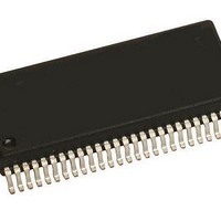
KIT33937AEKEVBE Freescale Semiconductor, KIT33937AEKEVBE Datasheet - Page 5

KIT33937AEKEVBE
Manufacturer Part Number
KIT33937AEKEVBE
Description
Power Management Modules & Development Tools 3-PHASE FET PRE-DRIV
Manufacturer
Freescale Semiconductor
Type
MOSFET & Power Driverr
Datasheet
1.MCZ33937AEKR2.pdf
(48 pages)
Specifications of KIT33937AEKEVBE
Interface Type
SPI
Product
Power Management Modules
Silicon Manufacturer
Freescale
Silicon Core Number
MC33937
Kit Application Type
Power Management
Application Sub Type
FET Driver
Kit Contents
Board, CD
Rohs Compliant
Yes
For Use With/related Products
MC33937
Table 2. 33937 Pin Definitions (continued)
Analog Integrated Circuit Device Data
Freescale Semiconductor
A functional description of each pin can be found in the
30, 31
Pin
12
13
14
15
16
17
18
19
20
21
22
23
24
25
26
27
28
29
32
34
35
36
37
38
39
40
41
42
43
44
AMP_OUT
PC_BOOT
PC_HS_G
PB_HS_G
PB_BOOT
Pin Name
VLS_CAP
PC_LS_G
PC_HS_S
PB_LS_G
PB_HS_S
PC_LS_S
PB_LS_S
PA_LS_S
OC_OUT
AMP_N
AMP_P
OC_TH
PA_HS
PB_HS
PC_HS
PA_LS
PB_LS
PC_LS
SCLK
VDD
GND
VSS
INT
CS
SO
SI
Analog Output
Analog Output
Analog Output VLS Regulator Output
Pin Function
Digital Output
Digital Output
Digital Output
Power Output Phase C Low Side Gate
Power Output
Power Output Phase B Low Side Gate
Power Output
Analog Input
Analog Input
Analog Input Over-current Threshold Threshold of the over-current detector
Analog Input
Analog Input
Digital Input
Digital Input
Digital Input
Digital Input
Digital Input
Digital Input
Digital Input
Digital Input
Digital Input
Power Input
Power Input
Power Input
Power Input
Power Input
Ground
Ground
Voltage Source Supply Ground reference for logic interface and power supplies
Amplifier Non-Invert
Phase C High Side
Phase C High Side
Phase C High Side
Phase A High Side
Phase B High Side
Phase C Bootstrap
Phase B High Side
Phase B High Side
Phase B Bootstrap
Phase A Low Side
Phase B Low Side
Phase C Low Side
Phase C Low Side
Phase B Low Side
Phase A Low Side
Over-current Out
Amplifier Output
VDD Regulator
Amplifier Invert
Formal Name
Serial Clock
Chip Select
Gate Drive
Gate Drive
Serial Out
Capacitor
Interrupt
Serial In
Ground
Source
Source
Source
Source
Source
Drive
Drive
Functional Pin Description
Active low input logic signal enables the High Side Driver for Phase A
Active high input logic signal enables the Low Side Driver for Phase A
VDD regulator output capacitor connection.
Active low input logic signal enables the High Side Driver for Phase B
Active high input logic signal enables the Low Side Driver for Phase B
Interrupt pin output
Chip Select input. It frames SPI commands and enables SPI port
Input data for SPI port. Clocked on the falling edge of SCLK, MSB first
Clock for SPI port and typically is 3.0 MHz
Output data for SPI port. Tri-state until CS becomes low
Active high input logic signal enables the Low Side Driver for Phase C
Active low input logic signal enables the High Side Driver for Phase C
Output of the current-sensing amplifier
Inverting input of the current-sensing amplifier
Non-inverting input of the current-sensing amplifier
Totem pole digital output of the Over-current Comparator
Substrate and ESD reference, connect to VSS
VLS Regulator connection for additional output capacitor, providing low
impedance supply source for Low Side Gate Drive
Source connection for Phase C Low Side FET
Gate drive output for Phase C Low Side
Source connection for Phase C High Side FET
Gate Drive for output Phase C High Side FET
Bootstrap capacitor for Phase C
Source connection for Phase B Low Side FET
Gate Drive for output Phase B Low Side
Source connection for Phase B High Side FET
Gate Drive for output Phase B High Side
Bootstrap capacitor for Phase B
Source connection for Phase A Low Side FET
section beginning on
Definition
page
PIN CONNECTIONS
23.
33937
5


