KIT33912EVME Freescale Semiconductor, KIT33912EVME Datasheet - Page 29
KIT33912EVME
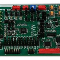
Manufacturer Part Number
KIT33912EVME
Description
MCU, MPU & DSP Development Tools For MC33912 RS-232 SPI
Manufacturer
Freescale Semiconductor
Datasheet
1.KIT33912EVME.pdf
(50 pages)
Specifications of KIT33912EVME
Processor To Be Evaluated
MC33912
Interface Type
RS-232, SPI
Operating Supply Voltage
12 V
Lead Free Status / RoHS Status
Lead free / RoHS Compliant


If a PDU is not completely filled, the unused bytes are filled with ones, meaning that their value will be 255 (0xFF). This is
necessary since a user defined diagnostic frame is always eight bytes long.
6.2.2 CMD data interpretation
Freescale Semiconductor
SPI
The SPI command will perform the “ReadWriteSPI8bit(addr + data)” function of the embedded software, returning the SPI
status data structure. This function waits for the LIN response frame.
This command only uses the M0 and S0 bytes. The message structure is described as follows:
PWM
PWM commands transmit data to the pulse width modulation registers in the MCU. To adjust the pulse width modulation
requires the frequency, duty cycle and range of the MCU clock prescaler. Values of the frequency and duty cycle are
separated into two bytes.
This command uses bytes M0, M1, M2, M3, M4. The message structure is described as follows:
ADC
ADC commands announce a data read from the A/D converter. After receiving a frame with the CMD value equal to ADC,
the response frame waits to transmit the value from the A/D converter register, which is separated into two bytes.
This command uses bytes S0, S1, S2 and S3. The message structure is described as follows:
M0 - M5
S0 - S5
Request
Response
Request
Response - No response.
Data being sent by the master in a request. The meaning of the data is related to the CMD. It will be described in
the next section.
Status data sent in a response by an addressed slave. The meaning of the data is related to the CMD. It will be
described in the next section.
M0 - SPI request
M1 - 0xFF
M2 - 0xFF
M3 - 0xFF
M4 - 0xFF
M5 - 0xFF
S0 - SPI response
S1 - 0xFF
S2 - 0xFF
S3 - 0xFF
S4 - 0xFF
S5 - 0xFF
M0 - lower part of value appointed to the frequency register
M1 - upper part of value appointed to the frequency register
M2 - lower part of value appointed to the duty register
M3 - upper part of value appointed to the duty register
M4 - value of the range appointed to change the MCU clock prescaler
M5 - 0xFF
KIT33912EVME System Basis Chip with LIN Tranceiver Setup Instructions, Rev. 2.0
Embedded Slave Software
21
Related parts for KIT33912EVME
Image
Part Number
Description
Manufacturer
Datasheet
Request
R

Part Number:
Description:
Manufacturer:
Freescale Semiconductor, Inc
Datasheet:
Part Number:
Description:
Manufacturer:
Freescale Semiconductor, Inc
Datasheet:
Part Number:
Description:
Manufacturer:
Freescale Semiconductor, Inc
Datasheet:
Part Number:
Description:
Manufacturer:
Freescale Semiconductor, Inc
Datasheet:
Part Number:
Description:
Manufacturer:
Freescale Semiconductor, Inc
Datasheet:
Part Number:
Description:
Manufacturer:
Freescale Semiconductor, Inc
Datasheet:
Part Number:
Description:
Manufacturer:
Freescale Semiconductor, Inc
Datasheet:
Part Number:
Description:
Manufacturer:
Freescale Semiconductor, Inc
Datasheet:
Part Number:
Description:
Manufacturer:
Freescale Semiconductor, Inc
Datasheet:
Part Number:
Description:
Manufacturer:
Freescale Semiconductor, Inc
Datasheet:
Part Number:
Description:
Manufacturer:
Freescale Semiconductor, Inc
Datasheet:
Part Number:
Description:
Manufacturer:
Freescale Semiconductor, Inc
Datasheet:
Part Number:
Description:
Manufacturer:
Freescale Semiconductor, Inc
Datasheet:
Part Number:
Description:
Manufacturer:
Freescale Semiconductor, Inc
Datasheet:
Part Number:
Description:
Manufacturer:
Freescale Semiconductor, Inc
Datasheet: