AP602-PCB900 TriQuint, AP602-PCB900 Datasheet
AP602-PCB900
Specifications of AP602-PCB900
Available stocks


Related parts for AP602-PCB900


AP602-PCB900 Summary of contents
Page 1
... Rating -55 to +125 ºC Ordering Information 192 ºC Part No. Input P6dB 0.1 mA AP602 0.1 mA AP602-PCB900 160 mA AP602-PCB1960 1930-1990 MHz Evaluation board 4.7 W AP602-PCB2140 2110-2170 MHz Evaluation board Functional Diagram The device ACLR1 vs. Output Power vs. Vcc WCDMA, Icq = 80 mA, 2140 MHz, 25 ˚C ...
Page 2
... AP602 High Dynamic Range 4W 28V HBT Amplifier S-Parameters ( Gain / Maximum Stable Gain 40 DB(|S(2,1)|) -10 0 0.5 1 1.5 Frequency (GHz) The gain for the unmatched device in 50 ohm system is shown as the trace in black color. For a tuned circuit for a particular frequency expected that actual gain will be higher the maximum stable gain. The maximum stable gain is shown in the marked red line. ...
Page 3
... Vpd is used as a reference for the internal active bias circuitry. It can be used to turn on/off the amplifier. Ipd depends on the Icq quiescent current setting. Ipd can 4mA at a quiescent current setting of 160mA. 3. Vbias should be maintained fixed at +5V. Ibias will change based on RF input power level. It can 4mA on the AP602 ...
Page 4
... AP602 High Dynamic Range 4W 28V HBT Amplifier 869-960 Application Circuit (AP602-PCB900) Typical WCDMA Performance at 25 ° channel power of +27 dBm Frequency 940 MHz W-CDMA Channel Power +27 dBm Power Gain 15.5 dB Input Return Loss 11 dB Output Return Loss 6.4 dB ACLR -50 dBc IMD3 @ +27 dBm PEP ...
Page 5
... The center placed at 0.135” (11.5° @ 1960 MHz) from the edge of the AP602 (U1). 5. The center of C30 is placed at 0.580” (49.6° @ 1960 MHz) from the edge of the AP602 (U1). 6. The bold-faced RF trace is for the DC bias feed. The stub’s length is approximately a ¼ λ. ...
Page 6
... The center placed at 0.135” (11.8° @ 2015 MHz) from the edge of the AP602 (U1). 5. The center of C30 is placed at 0.530” (50.9° @ 2015 MHz) from the edge of the AP602 (U1). 6. The bold-faced RF trace is for the DC bias feed. The stub’s length is approximately a ¼ λ. ...
Page 7
... The center placed at 0.035” (3.26° @ 2140 MHz) from the edge of the AP602 (U1). 6. The center placed at 0.510” (47.6° @ 2140 MHz) from the edge of the AP602 (U1). 7. The bold-faced RF trace is for the DC bias feed. The stub’s length is approximately a ¼ λ. ...
Page 8
... AP602 High Dynamic Range 4W 28V HBT Amplifier 2110-2170 MHz Application Circuit Performance Plots W-CDMA 3GPP Test Model 1+64 DPCH, 60% clipping, PAR = 8 0.01% Probability, 3.84 MHz BW Gain vs. Output Power vs. Temperature CW tone, Vcc = 28V, Icq = 80 mA, 2140 MHz -40 ˚C 25 ˚ ˚ Output Power (dBm) ACLR1 vs ...
Page 9
... High Dynamic Range 4W 28V HBT Amplifier 2110-2170 MHz Application Note: Changing Icq Biasing Configurations The AP602 can be configured to operate with lower bias current by varying the bias-adjust resistor – R2. The recommended circuit configurations shown previously in this datasheet have the device operating with the quiescent current (I This biasing level represents the best tradeoff in terms of linearity and efficiency ...
Page 10
... The center placed at 0.050” (5.1° @ 2.35 GHz) from the edge of the AP602 (U1). 4. The center of C28 is placed at 0.130” (13.3° @ 2.35 GHz) from the edge of the AP602 (U1). 5. The center of C29 is placed at 0.110” (11.3° @ 2.35 GHz) from the center of C28. ...
Page 11
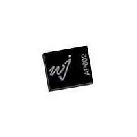
... Junction Temperature (°C) Product Marking The component will be laser marked with an “AP602-F” product label with an alphanumeric lot code on the top surface of the package. Tape and reel specifications for this part will be located on the website in the “Application Notes” section. ...