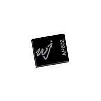
AP602-PCB900 TriQuint, AP602-PCB900 Datasheet - Page 9

AP602-PCB900
Manufacturer Part Number
AP602-PCB900
Description
RF Modules & Development Tools 869-960MHz Eval Brd 15.5dB Gain
Manufacturer
TriQuint
Datasheet
1.AP602-PCB900.pdf
(11 pages)
Specifications of AP602-PCB900
Board Size
6 mm x 5 mm x 1 mm
Minimum Frequency
869 MHz
Minimum Operating Temperature
- 40 C
Supply Voltage (min)
28 V
Product
RF Development Tools
Maximum Frequency
960 MHz
Output Power
4 W
Supply Voltage (max)
80 V
Supply Current
112 mA
Maximum Operating Temperature
+ 85 C
For Use With/related Products
AP602
Lead Free Status / RoHS Status
Lead free / RoHS Compliant
Other names
1067319
Available stocks
Company
Part Number
Manufacturer
Quantity
Price
Part Number:
AP602-PCB900
Manufacturer:
WJ
Quantity:
20 000
WJ Communications, Inc • Phone 1-800-WJ1-4401 • FAX: 408-577-6621 • e-mail: sales@wj.com • Web site: www.wj.com, www.TriQuint.com
The AP602 can be configured to operate with lower bias current by varying the bias-adjust resistor – R2. The recommended
circuit configurations shown previously in this datasheet have the device operating with a 80 mA as the quiescent current (I
This biasing level represents the best tradeoff in terms of linearity and efficiency. Lowering I
efficiency of the device, but degraded linearity. Increasing I
the device’s efficiency. Measured data shown in the plots below represents the AP602 measured and configured for 2.14 GHz
applications. It is expected that variation of the bias current for other frequency applications will produce similar performance
results.
(mA)
100
120
140
160
Icq
20
40
60
80
55
50
45
40
35
30
2110-2170 MHz Application Note: Changing Icq Biasing Configurations
-35
-40
-45
-50
-55
-60
-65
16
15
14
13
12
11
24
20
19
(ohms)
CW 2-tone signal, 2140 MHz, ∆f = 1 MHz, Vcc = 28V, 25 ˚C
6.00k
2.76k
1.80k
1.33k
1.05k
859
723
621
R2
20 mA
100 mA
20 mA
100 mA
AP602
High Dynamic Range 4W 28V HBT Amplifier
26
OIP3 vs. Output Power vs. Icq
ACLR1 vs. Output Power vs. Icq
21
Average Output Power (dBm)
Gain vs. Output Power vs. Icq
Output Power, PEP (dBm)
24
CW tone, Vcc = 28V, 2140 MHz, 25 ˚C
WCDMA, Vcc = 28V, 2140 MHz, 25 ˚C
Output Power (dBm)
V
(V)
40 mA
120 mA
28
40 mA
120 mA
5
5
5
5
5
5
5
5
PD
23
28
PIN_V
30
25
60 mA
140 mA
2.53
2.61
2.67
2.73
2.79
2.84
2.89
2.94
60 mA
140 mA
(V)
20 mA
60 mA
100 mA
140 mA
32
PD
32
27
80 mA
160 mA
80 mA
160 mA
40 mA
80 mA
120 mA
160 mA
34
80
60
40
20
29
36
0
17
36
32
28
24
20
-30
-40
-50
-60
-70
-80
20 mA
40 mA
60 mA
80 mA
100 mA
120 mA
140 mA
160 mA
200
150
100
Thermal Rise vs. Output Power vs. Icq
50
19
0
8
24
19
20 mA
60 mA
100 mA
140 mA
CW 2-tone signal, 2140 MHz, ∆f = 1 MHz, Vcc = 28V, 25 ˚C
Output Power (dBm)
Output Power vs. Input Power vs. Icq
21
26
IMD3 vs. Output Power vs. Icq
21
12
Icc vs. Output Power vs. Icq
Average Output Power (dBm)
CW tone, Vcc = 28V, 2140 MHz, 25 ˚C
WCDMA, Vcc = 28V, 2140 MHz, 25 ˚C
Output Power, PEP (dBm)
20 mA
100 mA
40 mA
80 mA
120 mA
160 mA
Vcc = 28V
20 mA
100 mA
Input Power (dBm)
23
CQ
28
23
has nominal improvement upon the linearity, but will degrade
40 mA
120 mA
16
40 mA
120 mA
25
30
25
27
60 mA
140 mA
60 mA
140 mA
20
32
27
29
80 mA
160 mA
80 mA
160 mA
29
24
34
Specifications and information are subject to change without notice
C22
0.5 pF
See note 5
See note 4
50
40
30
20
10
30
25
20
15
10
0
-30
-40
-50
-60
-70
-80
5
0
20
19
24
20 mA
60 mA
100 mA
140 mA
20 mA
60 mA
100 mA
140 mA
CW 2-tone signal, 2140 MHz, ∆f = 1 MHz, Vcc = 28V, 25 ˚C
20 mA
100 mA
1000 pF
Efficiency vs. Output Power vs. Icq
Efficiency vs. Output Power vs. Icq
See note 3
21
26
100pF
Average Output Power (dBm)
C7
24
WCDMA, Vcc = 28V, 2140 MHz, 25 ˚C
CW tone, Vcc = 28V, 2140 MHz, 25 ˚C
IMD5 vs. Output Power vs. Icq
40 mA
80 mA
120 mA
160 mA
Output Power, PEP (dBm)
Output Power (dBm)
CQ
40 mA
120 mA
40 mA
80 mA
120 mA
160 mA
23
will improve upon the
28
28
Page 9 of 11 May 2007 ver 1
60 mA
140 mA
25
30
W = .030”
L = .980”
See note 6
80 mA
160 mA
32
27
32
CQ
29
36
34
).


