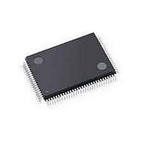
DAC1405D750HW/C1,551 NXP Semiconductors, DAC1405D750HW/C1,551 Datasheet - Page 14

DAC1405D750HW/C1,551
Manufacturer Part Number
DAC1405D750HW/C1,551
Description
DAC (D/A Converters) Dual 14BtDAC 750Msps 4xand 8xnterpolating
Manufacturer
NXP Semiconductors
Datasheet
1.DAC1405D650HWC15.pdf
(45 pages)
Specifications of DAC1405D750HW/C1,551
Number Of Dac Outputs
4
Conversion Rate
650 MSPS
Resolution
14 bit
Supply Voltage (max)
3.6 V
Supply Voltage (min)
3 V
Maximum Operating Temperature
+ 85 C
Mounting Style
SMD/SMT
Maximum Power Dissipation
0.53 W
Minimum Operating Temperature
- 40 C
Supply Current
5 mA
Number Of Converters
2
Settling Time
20 ns
Package / Case
HTQFP-100
Lead Free Status / RoHS Status
Lead free / RoHS Compliant
Other names
935290796551
NXP Semiconductors
DAC1405D650
Product data sheet
Fig 3.
RESET_N
(optional)
SCS_N
SCLK
SDIO
SDO
R/W indicates the mode access, (see
SPI protocol
10.2.2 SPI timing description
R/W
Table 6.
In
byte.
Table 7.
A[4:0]: indicates which register is being addressed. In the case of a multiple transfer, this
address concerns the first register after which the next registers follow directly in a
decreasing order according to
The SPI interface can operate at a frequency of up to 15 MHz. The SPI timing is shown in
Figure
R/W
0
1
N1
0
0
1
1
N1
Table 7
N0
4.
below N1 and N0 indicate the number of bytes transferred after the instruction
Read or Write mode access description
Number of bytes to be transferred
A4
All information provided in this document is subject to legal disclaimers.
A3
Table
Description
Write mode operation
Read mode operation
N0
0
1
0
1
Rev. 3 — 10 September 2010
6):
A2
Dual 14-bit DAC, up to 650 Msps; 2×, 4× and 8× interpolating
A1
Table 9 “Register allocation
A0
D7
D7
Number of bytes
1 byte transferred
2 bytes transferred
3 bytes transferred
4 bytes transferred
D6
D6
D5
D5
D4
D4
map”.
DAC1405D650
D3
D3
D2
D2
© NXP B.V. 2010. All rights reserved.
D1
D1
D0
D0
001aaj812
14 of 45


