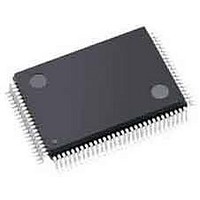
ispPAC-POWR1220AT8-02TN100I Lattice, ispPAC-POWR1220AT8-02TN100I Datasheet - Page 41

ispPAC-POWR1220AT8-02TN100I
Manufacturer Part Number
ispPAC-POWR1220AT8-02TN100I
Description
Current & Power Monitors & Regulators Prec. Power Supply Seq. Monitor Marg.
Manufacturer
Lattice
Series
ispPAC®r
Datasheet
1.ISPPAC-POWR1220AT8-02TN100I.pdf
(54 pages)
Specifications of ispPAC-POWR1220AT8-02TN100I
Mounting Style
SMD/SMT
Supply Voltage (max)
3.96 V
Supply Voltage (min)
2.8 V
Package / Case
TQFP-100
Applications
General Purpose
Voltage - Input
-0.3 V ~ 5.9 V
Voltage - Supply
2.8 V ~ 3.96 V
Current - Supply
40mA
Operating Temperature
-40°C ~ 85°C
Mounting Type
Surface Mount
Lead Free Status / RoHS Status
Lead free / RoHS Compliant
Available stocks
Company
Part Number
Manufacturer
Quantity
Price
Company:
Part Number:
ISPPAC-POWR1220AT8-02TN100I
Manufacturer:
Lattice
Quantity:
226
Company:
Part Number:
ISPPAC-POWR1220AT8-02TN100I
Manufacturer:
Lattice Semiconductor Corporation
Quantity:
10 000
Lattice Semiconductor
ispPAC-POWR1220AT8 Data Sheet
2
Designs using the SMBAlert feature are required to set the device’s I
C/SMBus address to the lowest of all the
2
addresses on that I
C/SMBus.
Software-Based Design Environment
Designers can configure the ispPAC-POWR1220AT8 using PAC-Designer, an easy to use, Microsoft Windows
compatible program. Circuit designs are entered graphically and then verified, all within the PAC-Designer environ-
ment. Full device programming is supported using PC parallel port I/O operations and a download cable connected
to the serial programming interface pins of the ispPAC-POWR1220AT8. A library of configurations is included with
basic solutions and examples of advanced circuit techniques are available on the Lattice web site for downloading.
In addition, comprehensive on-line and printed documentation is provided that covers all aspects of PAC-Designer
operation. The PAC-Designer schematic window, shown in Figure 1-33, provides access to all configurable ispPAC-
POWR1220AT8 elements via its graphical user interface. All analog input and output pins are represented. Static or
non-configurable pins such as power, ground, and the serial digital interface are omitted for clarity. Any element in
the schematic window can be accessed via mouse operations as well as menu commands. When completed, con-
figurations can be saved, simulated, and downloaded to devices.
Figure 1-33. PAC-Designer ispPAC-POWR1220AT8 Design Entry Screen
In-System Programming
2
The ispPAC-POWR1220AT8 is an in-system programmable device. This is accomplished by integrating all E
con-
figuration memory and control logic on-chip. Programming is performed through a 4-wire, IEEE 1149.1 compliant
serial JTAG interface at normal logic levels. Once a device is programmed, all configuration information is stored
2
on-chip, in non-volatile E
CMOS memory cells. The specifics of the IEEE 1149.1 serial interface and all ispPAC-
POWR1220AT8 instructions are described in the JTAG interface section of this data sheet.
1-41


