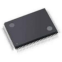
ispPAC-POWR1220AT8-02TN100I Lattice, ispPAC-POWR1220AT8-02TN100I Datasheet - Page 6

ispPAC-POWR1220AT8-02TN100I
Manufacturer Part Number
ispPAC-POWR1220AT8-02TN100I
Description
Current & Power Monitors & Regulators Prec. Power Supply Seq. Monitor Marg.
Manufacturer
Lattice
Series
ispPAC®r
Datasheet
1.ISPPAC-POWR1220AT8-02TN100I.pdf
(54 pages)
Specifications of ispPAC-POWR1220AT8-02TN100I
Mounting Style
SMD/SMT
Supply Voltage (max)
3.96 V
Supply Voltage (min)
2.8 V
Package / Case
TQFP-100
Applications
General Purpose
Voltage - Input
-0.3 V ~ 5.9 V
Voltage - Supply
2.8 V ~ 3.96 V
Current - Supply
40mA
Operating Temperature
-40°C ~ 85°C
Mounting Type
Surface Mount
Lead Free Status / RoHS Status
Lead free / RoHS Compliant
Available stocks
Company
Part Number
Manufacturer
Quantity
Price
Company:
Part Number:
ISPPAC-POWR1220AT8-02TN100I
Manufacturer:
Lattice
Quantity:
226
Company:
Part Number:
ISPPAC-POWR1220AT8-02TN100I
Manufacturer:
Lattice Semiconductor Corporation
Quantity:
10 000
Lattice Semiconductor
Absolute Maximum Ratings
Absolute maximum ratings are shown in the table below. Stresses beyond those listed may cause permanent dam-
age to the device. Functional operation of the device at these or any other conditions beyond those indicated in the
recommended operating conditions of this specification is not implied.
Recommended Operating Conditions
ESD Performance
V
V
V
V
V
V
V
V
V
I
T
T
1. The VCCPROG pin MUST be left floating when VCCD and VCCA are powered.
V
V
V
V
V
V
V
V
T
T
SINKMAXTOTAL
A
APROG
A
S
CCD,
CCINP
CCJ
CCPROG
IN
MON
MONGS
OUT
CCD
CCA
CCINP
CCJ
CCPROG
IN
MON+
MONGS
TRI
Symbol
Symbol
V
CCA
1
Core supply voltage at pin
Digital input supply for IN[1:6] at pin
JTAG logic supply voltage at pin
Alternate E
Input voltage at digital input pins
Input voltage at V
Input voltage at V
Open-drain output voltage
Ambient temperature during
programming
Ambient temperature
All pins
Core supply
Analog supply
Digital input supply (IN[1:6])
JTAG logic supply
Alternate E
Digital input voltage (all digital I/O pins)
V
V
Voltage applied to tri-stated pins
Maximum sink current on any output
Storage temperature
Ambient temperature
MON
MON
Pin Group
input voltage
input voltage ground sense
2
programming supply at pin
Parameter
2
programming supply
MON
MONGS
Parameter
pins
pins
ESD Stress
CDM
HBM
1
V
V
OUT[5:20] pins
HVOUT[1:4] pins in open-drain
mode
Power applied
CCD
CCD
1-6
and V
and V
Conditions
HVOUT[1:4]
OUT[5:20]
CCA
CCA
2000
Conditions
1000
Min.
powered
not powered
ispPAC-POWR1220AT8 Data Sheet
Must Be Left Floating
Min.
Min.
2.25
2.25
-0.5
-0.5
-0.5
-0.5
-0.5
-0.5
-0.5
-0.5
-0.5
-0.5
Units
-0.3
-0.3
-0.2
-0.3
-0.3
-65
-65
2.8
3.0
-40
-40
V
V
No Connect
Max.
Max.
13.3
3.96
13.0
150
125
4.5
4.5
5.5
3.6
3.6
5.5
5.9
0.3
5.5
23
85
85
6
6
4
6
6
6
6
Units
Units
mA
o
o
o
o
V
V
V
V
V
V
V
V
V
V
V
V
V
V
V
V
V
V
V
C
C
C
C


