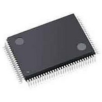
ispPAC-POWR1220AT8-02TN100I Lattice, ispPAC-POWR1220AT8-02TN100I Datasheet - Page 8

ispPAC-POWR1220AT8-02TN100I
Manufacturer Part Number
ispPAC-POWR1220AT8-02TN100I
Description
Current & Power Monitors & Regulators Prec. Power Supply Seq. Monitor Marg.
Manufacturer
Lattice
Series
ispPAC®r
Datasheet
1.ISPPAC-POWR1220AT8-02TN100I.pdf
(54 pages)
Specifications of ispPAC-POWR1220AT8-02TN100I
Mounting Style
SMD/SMT
Supply Voltage (max)
3.96 V
Supply Voltage (min)
2.8 V
Package / Case
TQFP-100
Applications
General Purpose
Voltage - Input
-0.3 V ~ 5.9 V
Voltage - Supply
2.8 V ~ 3.96 V
Current - Supply
40mA
Operating Temperature
-40°C ~ 85°C
Mounting Type
Surface Mount
Lead Free Status / RoHS Status
Lead free / RoHS Compliant
Available stocks
Company
Part Number
Manufacturer
Quantity
Price
Company:
Part Number:
ISPPAC-POWR1220AT8-02TN100I
Manufacturer:
Lattice
Quantity:
226
Company:
Part Number:
ISPPAC-POWR1220AT8-02TN100I
Manufacturer:
Lattice Semiconductor Corporation
Quantity:
10 000
Lattice Semiconductor
Margin/Trim DAC Output Characteristics
ADC Characteristics
ADC Error Budget Across Entire Operating Temperature Range
FSR
LSB
I
BPZ
TS
C_LOAD
T
TOSE
1. To 1% of set value with 50pf load connected to trim pins.
2. Total time required to update a single TRIMx output value by setting the associated DAC through the I
3. This is the total resultant error in the trimmed power supply output voltage referred to any DAC code due to the DAC’s INL, DNL, gain, out-
T
V
ADC Step Size LSB
Eattenuator
1. Maximum voltage is limited by V
TADC Error
1. Total error, guaranteed by characterization, includes INL, DNL, Gain, Offset, and PSR specs of the ADC.
OUT
UPDATEM
CONVERT
IN
put impedance, offset error and bipolar offset error across the industrial temperature range and the ispPAC-POWR1200AT8 operating V
and V
Symbol
Symbol
Symbol
CCD
ranges.
Resolution
Full scale range
LSB step size
Output source/sink current
Bipolar zero output voltage
(code=80h)
TrimCell output voltage settling
time
Maximum load capacitance
Update time through I
Total open loop supply voltage
error
ADC Resolution
Conversion Time
Input range Full Scale
Error Due to Attenuator
Total Measurement Error at
Any Voltage
1
3
Parameter
Parameter
Parameter
1
MONX
pin (theoretical maximum is 6.144V).
2
C port
2
Time from I
Programmable Attenuator = 1
Programmable Attenuator = 3
Programmable Attenuator = 1
Programmable Attenuator = 3
Programmable Attenuator = 3
Measurement Range 600 mV - 2.048V,
VMONxGS > -100mV, Attenuator =1
Measurement Range 600 mV - 2.048V,
VMONxGS > -200mV, Attenuator =1
Measurement Range 0 - 2.048V,
VMONxGS > -200mV, Attenuator =1
Offset 1
Offset 2
Offset 3
Offset 4
DAC code changed
from 80H to FFH or
80H to 00H
Single DAC code
change
MCLK = 8MHz
Full scale DAC corre-
sponds to ±5% supply
voltage variation
Conditions
2
1-8
C Request
Conditions
Conditions
ispPAC-POWR1220AT8 Data Sheet
-200
-1%
Min
8(7+sign)
+/-320
Min.
Min.
1.25
Typ
256
260
2.5
0.6
0.8
1.0
2
-8
C port.
0
0
+/- 0.1
+/-10
Typ.
Typ.
+/-4
+/-6
10
2
6
+1%
Max
200
2.5
50
2.048
Max.
Max.
200
5.9
8
1
Units
V/V
bits
mV
mV
ms
µA
µs
pF
µs
Units
Units
V
Bits
mV
mV
mV
mV
mV
µs
%
V
V
CCA


