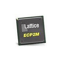
LFE2-12E-5FN256C Lattice, LFE2-12E-5FN256C Datasheet - Page 21

LFE2-12E-5FN256C
Manufacturer Part Number
LFE2-12E-5FN256C
Description
FPGA - Field Programmable Gate Array 12K LUTs 193 I/O DSP 1.2V -5 Spd
Manufacturer
Lattice
Datasheet
1.LFE2-12SE-6FN256C.pdf
(389 pages)
Specifications of LFE2-12E-5FN256C
Number Of Macrocells
12000
Number Of Programmable I/os
193
Data Ram Size
226304
Supply Voltage (max)
1.26 V
Maximum Operating Temperature
+ 85 C
Minimum Operating Temperature
0 C
Mounting Style
SMD/SMT
Supply Voltage (min)
1.14 V
Package / Case
FPBGA-256
No. Of Logic Blocks
12000
No. Of Macrocells
6000
No. Of Speed Grades
5
Total Ram Bits
221Kbit
No. Of I/o's
193
Clock Management
DLL, PLL
I/o Supply Voltage
3.465V
Rohs Compliant
Yes
Lead Free Status / RoHS Status
Lead free / RoHS Compliant
Available stocks
Company
Part Number
Manufacturer
Quantity
Price
Company:
Part Number:
LFE2-12E-5FN256C
Manufacturer:
Lattice
Quantity:
135
Company:
Part Number:
LFE2-12E-5FN256C
Manufacturer:
LG
Quantity:
6 317
Company:
Part Number:
LFE2-12E-5FN256C
Manufacturer:
Lattice Semiconductor Corporation
Quantity:
10 000
- Current page: 21 of 389
- Download datasheet (5Mb)
Lattice Semiconductor
Figure 2-18. Slice0 through Slice2 Control Selection
Edge Clock Routing
LatticeECP2/M devices have a number of high-speed edge clocks that are intended for use with the PIOs in the
implementation of high-speed interfaces. There are eight edge clocks per device: two edge clocks per edge. Differ-
ent PLL and DLL outputs are routed to the two muxes on the left and right sides of the device. In addition, the
CLKO signal (generated from the DLLDELA block) is routed to all the edge clock muxes on the left and right sides
of the device. Figure 2-19 shows the selection muxes for these clocks.
Figure 2-19. Edge Clock Mux Connections
Secondary Clock
GPLL Output CLKOP
GPLL Output CLKOS
DLL Output CLKOP
DLL Output CLKOS
Clock Input Pad
GPLL Input Pad
GPLL Input Pad
Routing
Vcc
Input Pad
Input Pad
Routing
Routing
Routing
CLKO
CLKO
12
3
1
2-18
16:1
Top and Bottom
ECLK1/ ECLK2
Left and Right
Left and Right
Edge Clocks
Edge Clocks
Edge Clocks
(Both Mux)
LatticeECP2/M Family Data Sheet
ECLK1
ECLK2
Slice Control
Architecture
Related parts for LFE2-12E-5FN256C
Image
Part Number
Description
Manufacturer
Datasheet
Request
R

Part Number:
Description:
FPGA - Field Programmable Gate Array 12K LUTs 93 I/O DSP 1.2V -5 Spd
Manufacturer:
Lattice
Datasheet:

Part Number:
Description:
FPGA - Field Programmable Gate Array 12K LUTs 93 I/O DSP 1.2V -5 Spd I
Manufacturer:
Lattice

Part Number:
Description:
FPGA - Field Programmable Gate Array 12K LUTs 131 I/O DSP 1.2V -5 Spd
Manufacturer:
Lattice

Part Number:
Description:
FPGA - Field Programmable Gate Array 12K LUTs 93 I/O DSP 1.2V -5 Spd
Manufacturer:
Lattice

Part Number:
Description:
FPGA - Field Programmable Gate Array 12K LUTs 131 I/O DSP 1.2V -5 Spd I
Manufacturer:
Lattice

Part Number:
Description:
FPGA - Field Programmable Gate Array 12K LUTs 193 I/O DSP 1.2V -5 Spd I
Manufacturer:
Lattice
Part Number:
Description:
IC, LATTICEECP2 FPGA, 420MHZ, FPBGA-256
Manufacturer:
LATTICE SEMICONDUCTOR
Datasheet:

Part Number:
Description:
IC, LATTICEECP2 FPGA, 420MHZ, QFP-208
Manufacturer:
LATTICE SEMICONDUCTOR
Datasheet:

Part Number:
Description:
IC, LATTICEECP2 FPGA, 420MHZ, TQFP-144
Manufacturer:
LATTICE SEMICONDUCTOR
Datasheet:
Part Number:
Description:
FPGA LatticeECP2 Family 12000 Cells 90nm (CMOS) Technology 1.2V 256-Pin FBGA
Manufacturer:
LATTICE SEMICONDUCTOR
Datasheet:
Part Number:
Description:
FPGA LatticeECP2 Family 12000 Cells 90nm (CMOS) Technology 1.2V 256-Pin FBGA
Manufacturer:
LATTICE SEMICONDUCTOR
Datasheet:
Part Number:
Description:
FPGA LatticeECP2 Family 12000 Cells 90nm (CMOS) Technology 1.2V 484-Pin FBGA
Manufacturer:
LATTICE SEMICONDUCTOR
Datasheet:
Part Number:
Description:
FPGA LatticeECP2 Family 12000 Cells 90nm (CMOS) Technology 1.2V 256-Pin FBGA
Manufacturer:
LATTICE SEMICONDUCTOR
Datasheet:

Part Number:
Description:
FPGA LatticeECP2 Family 12000 Cells 90nm (CMOS) Technology 1.2V 208-Pin PQFP
Manufacturer:
Lattice
Datasheet:

Part Number:
Description:
IC FPGA 12KLUTS 131I/O 208-BGA
Manufacturer:
Lattice
Datasheet:


