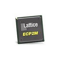
LFE2-12E-5FN256C Lattice, LFE2-12E-5FN256C Datasheet - Page 26

LFE2-12E-5FN256C
Manufacturer Part Number
LFE2-12E-5FN256C
Description
FPGA - Field Programmable Gate Array 12K LUTs 193 I/O DSP 1.2V -5 Spd
Manufacturer
Lattice
Datasheet
1.LFE2-12SE-6FN256C.pdf
(389 pages)
Specifications of LFE2-12E-5FN256C
Number Of Macrocells
12000
Number Of Programmable I/os
193
Data Ram Size
226304
Supply Voltage (max)
1.26 V
Maximum Operating Temperature
+ 85 C
Minimum Operating Temperature
0 C
Mounting Style
SMD/SMT
Supply Voltage (min)
1.14 V
Package / Case
FPBGA-256
No. Of Logic Blocks
12000
No. Of Macrocells
6000
No. Of Speed Grades
5
Total Ram Bits
221Kbit
No. Of I/o's
193
Clock Management
DLL, PLL
I/o Supply Voltage
3.465V
Rohs Compliant
Yes
Lead Free Status / RoHS Status
Lead free / RoHS Compliant
Available stocks
Company
Part Number
Manufacturer
Quantity
Price
Company:
Part Number:
LFE2-12E-5FN256C
Manufacturer:
Lattice
Quantity:
135
Company:
Part Number:
LFE2-12E-5FN256C
Manufacturer:
LG
Quantity:
6 317
Company:
Part Number:
LFE2-12E-5FN256C
Manufacturer:
Lattice Semiconductor Corporation
Quantity:
10 000
- Current page: 26 of 389
- Download datasheet (5Mb)
Lattice Semiconductor
MULT sysDSP Element
This multiplier element implements a multiply with no addition or accumulator nodes. The two operands, A and B,
are multiplied and the result is available at the output. The user can enable the input/output and pipeline registers.
Figure 2-23 shows the MULT sysDSP element.
Figure 2-23. MULT sysDSP Element
Multiplicand
Multiplier
Signed A
Signed B
Shift Register B Out
Shift Register B In
n
Input Data
Register B
n
n
n
Register
Register
Input
Input
m
Register A
Input Data
m
m
Shift Register A Out
m
Shift Register A In
2-23
Multiplier
Multiplier
m
n
To
To
Multiplier
Register
Pipeline
x
CLK (CLK0,CLK1,CLK2,CLK3)
CE (CE0,CE1,CE2,CE3)
RST(RST0,RST1,RST2,RST3)
LatticeECP2/M Family Data Sheet
(default)
m+n
m+n
Output
Architecture
Related parts for LFE2-12E-5FN256C
Image
Part Number
Description
Manufacturer
Datasheet
Request
R

Part Number:
Description:
FPGA - Field Programmable Gate Array 12K LUTs 93 I/O DSP 1.2V -5 Spd
Manufacturer:
Lattice
Datasheet:

Part Number:
Description:
FPGA - Field Programmable Gate Array 12K LUTs 93 I/O DSP 1.2V -5 Spd I
Manufacturer:
Lattice

Part Number:
Description:
FPGA - Field Programmable Gate Array 12K LUTs 131 I/O DSP 1.2V -5 Spd
Manufacturer:
Lattice

Part Number:
Description:
FPGA - Field Programmable Gate Array 12K LUTs 93 I/O DSP 1.2V -5 Spd
Manufacturer:
Lattice

Part Number:
Description:
FPGA - Field Programmable Gate Array 12K LUTs 131 I/O DSP 1.2V -5 Spd I
Manufacturer:
Lattice

Part Number:
Description:
FPGA - Field Programmable Gate Array 12K LUTs 193 I/O DSP 1.2V -5 Spd I
Manufacturer:
Lattice
Part Number:
Description:
IC, LATTICEECP2 FPGA, 420MHZ, FPBGA-256
Manufacturer:
LATTICE SEMICONDUCTOR
Datasheet:

Part Number:
Description:
IC, LATTICEECP2 FPGA, 420MHZ, QFP-208
Manufacturer:
LATTICE SEMICONDUCTOR
Datasheet:

Part Number:
Description:
IC, LATTICEECP2 FPGA, 420MHZ, TQFP-144
Manufacturer:
LATTICE SEMICONDUCTOR
Datasheet:
Part Number:
Description:
FPGA LatticeECP2 Family 12000 Cells 90nm (CMOS) Technology 1.2V 256-Pin FBGA
Manufacturer:
LATTICE SEMICONDUCTOR
Datasheet:
Part Number:
Description:
FPGA LatticeECP2 Family 12000 Cells 90nm (CMOS) Technology 1.2V 256-Pin FBGA
Manufacturer:
LATTICE SEMICONDUCTOR
Datasheet:
Part Number:
Description:
FPGA LatticeECP2 Family 12000 Cells 90nm (CMOS) Technology 1.2V 484-Pin FBGA
Manufacturer:
LATTICE SEMICONDUCTOR
Datasheet:
Part Number:
Description:
FPGA LatticeECP2 Family 12000 Cells 90nm (CMOS) Technology 1.2V 256-Pin FBGA
Manufacturer:
LATTICE SEMICONDUCTOR
Datasheet:

Part Number:
Description:
FPGA LatticeECP2 Family 12000 Cells 90nm (CMOS) Technology 1.2V 208-Pin PQFP
Manufacturer:
Lattice
Datasheet:

Part Number:
Description:
IC FPGA 12KLUTS 131I/O 208-BGA
Manufacturer:
Lattice
Datasheet:


