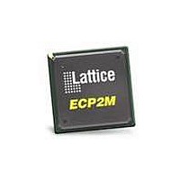
LFE2M20SE-5FN484C Lattice, LFE2M20SE-5FN484C Datasheet - Page 33

LFE2M20SE-5FN484C
Manufacturer Part Number
LFE2M20SE-5FN484C
Description
FPGA - Field Programmable Gate Array 19K LUTs 304 I/O S-Ser SERDES DSP -5
Manufacturer
Lattice
Datasheet
1.LFE2-12SE-6FN256C.pdf
(389 pages)
Specifications of LFE2M20SE-5FN484C
Number Of Macrocells
19000
Maximum Operating Frequency
311 MHz
Number Of Programmable I/os
304
Data Ram Size
1246208
Supply Voltage (max)
1.26 V
Maximum Operating Temperature
+ 85 C
Minimum Operating Temperature
0 C
Mounting Style
SMD/SMT
Supply Voltage (min)
1.14 V
Package / Case
FPBGA-484
Lead Free Status / RoHS Status
Lead free / RoHS Compliant
Available stocks
Company
Part Number
Manufacturer
Quantity
Price
Company:
Part Number:
LFE2M20SE-5FN484C
Manufacturer:
Lattice
Quantity:
135
Company:
Part Number:
LFE2M20SE-5FN484C
Manufacturer:
LATTICE
Quantity:
12
Company:
Part Number:
LFE2M20SE-5FN484C
Manufacturer:
Lattice Semiconductor Corporation
Quantity:
10 000
- Current page: 33 of 389
- Download datasheet (5Mb)
Lattice Semiconductor
Figure 2-28. PIC Diagram
Two adjacent PIOs can be joined to provide a differential I/O pair (labeled as “T” and “C”) as shown in Figure 2-28.
The PAD Labels “T” and “C” distinguish the two PIOs. Approximately 50% of the PIO pairs on the left and right
edges of the device can be configured as true LVDS outputs. All I/O pairs can operate as inputs.
DDRCLKPOL*
*Signals are available on left/right/bottom edges only.
** Selected blocks.
DQSXFER*
QNEG0*
QNEG1*
ONEG2*
QPOS0*
QPOS1*
OPOS2*
ONEG0
OPOS0
ONEG1
INDD
OPOS1
INCK**
ECLK1
ECLK2
IPOS0
IPOS1
GSRN
INFF
CLK
LSR
CE
TD
Control
Muxes
CLK1
CLK0
CEO
GSR
LSR
CEI
2-30
PIOA
Register
Register
Register
Tristate
Output
Block
Block
Block
Input
PIOB
IOLD0
IOLT0
DI
LatticeECP2/M Family Data Sheet
Buffer
sysIO
PADB
PADA
“C”
“T”
Architecture
Related parts for LFE2M20SE-5FN484C
Image
Part Number
Description
Manufacturer
Datasheet
Request
R

Part Number:
Description:
FPGA - Field Programmable Gate Array 19K LUTs 140 I/O S-Ser SERDES DSP -5
Manufacturer:
Lattice
Datasheet:
Part Number:
Description:
FPGA LatticeECP2M Family 19000 Cells 90nm (CMOS) Technology 1.2V 484-Pin FBGA
Manufacturer:
LATTICE SEMICONDUCTOR
Datasheet:

Part Number:
Description:
FPGA LatticeECP2M Family 19000 Cells 90nm (CMOS) Technology 1.2V 256-Pin FBGA
Manufacturer:
Lattice
Datasheet:

Part Number:
Description:
IC FPGA 20KLUTS 140I/O 256-BGA
Manufacturer:
Lattice
Datasheet:

Part Number:
Description:
IC FPGA 20KLUTS 140I/O 256-BGA
Manufacturer:
Lattice
Datasheet:

Part Number:
Description:
IC FPGA 20KLUTS 304I/O 484-BGA
Manufacturer:
Lattice
Datasheet:

Part Number:
Description:
IC FPGA 19KLUTS 484FGPBGA
Manufacturer:
Lattice
Datasheet:

Part Number:
Description:
FPGA - Field Programmable Gate Array 19K LUTs 304 I/O S-Ser SERD DSP -6
Manufacturer:
Lattice

Part Number:
Description:
FPGA - Field Programmable Gate Array 19K LUTs 304 I/O S-Ser SERD DSP -7
Manufacturer:
Lattice

Part Number:
Description:
FPGA - Field Programmable Gate Array 19K LUTs 140 I/O S-Ser SERD DSP -6 I
Manufacturer:
Lattice

Part Number:
Description:
FPGA - Field Programmable Gate Array 19K LUTs 140 I/O S-Ser SERD DSP -6
Manufacturer:
Lattice

Part Number:
Description:
FPGA - Field Programmable Gate Array 19K LUTs 304 I/O S-Ser SERDES DSP -5
Manufacturer:
Lattice

Part Number:
Description:
FPGA - Field Programmable Gate Array 19K LUTs 304 I/O S-Ser SERD DSP -6 I
Manufacturer:
Lattice


