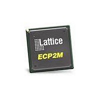
LFE2M20SE-5FN484C Lattice, LFE2M20SE-5FN484C Datasheet - Page 91

LFE2M20SE-5FN484C
Manufacturer Part Number
LFE2M20SE-5FN484C
Description
FPGA - Field Programmable Gate Array 19K LUTs 304 I/O S-Ser SERDES DSP -5
Manufacturer
Lattice
Datasheet
1.LFE2-12SE-6FN256C.pdf
(389 pages)
Specifications of LFE2M20SE-5FN484C
Number Of Macrocells
19000
Maximum Operating Frequency
311 MHz
Number Of Programmable I/os
304
Data Ram Size
1246208
Supply Voltage (max)
1.26 V
Maximum Operating Temperature
+ 85 C
Minimum Operating Temperature
0 C
Mounting Style
SMD/SMT
Supply Voltage (min)
1.14 V
Package / Case
FPBGA-484
Lead Free Status / RoHS Status
Lead free / RoHS Compliant
Available stocks
Company
Part Number
Manufacturer
Quantity
Price
Company:
Part Number:
LFE2M20SE-5FN484C
Manufacturer:
Lattice
Quantity:
135
Company:
Part Number:
LFE2M20SE-5FN484C
Manufacturer:
LATTICE
Quantity:
12
Company:
Part Number:
LFE2M20SE-5FN484C
Manufacturer:
Lattice Semiconductor Corporation
Quantity:
10 000
- Current page: 91 of 389
- Download datasheet (5Mb)
Lattice Semiconductor
Table 3-9. Channel Output Jitter - x20 Mode
Table 3-10. SERDES/PCS Latency Breakdown (Parallel Clock Cycle)
Deterministic
Random
Total
Deterministic
Random
Total
Deterministic
Random
Total
Note: Values are measured with PRBS 2
x20 mode.
Transmit Data Latency
Receive Data Latency
1. PCS internal parallel clock. This clock rate is the same as rxfullclk.
2. FPGA Bridge latency varies by the upsample/downsample FIFO read/write. The numbers given are for the 8b10b interface. The
3. 1 = -245ps, 2 = 700ps
Description
depth of the downsample/upsample FIFO is 4. The earliest read can be done after the write clock cycle (one clock) in downsample
FIFO. The latest read will be done after the FIFO is full (4 + 1 = 5). For the 16b20b interface, the numbers are doubled: min. = 2, max.
= 10. This latency depends on the internal FIFO flag operation.
Item
R1
T4
T1
T2
T3
R2
R3
R4
R5
R6
3
3
FPGA Bridge Transmit
8b10b Encoder
SERDES Bridge Transmit
Serializer: 8-bit mode
Serializer: 10-bit mode
Deserializer: 8-bit mode
Deserializer: 10-bit mode
SERDES Bridge Receive
Word Alignment
8b10b Decoder
Clock Tolerance Compensation
FPGA Bridge Receive
3.125 Gbps
3.125 Gbps
3.125 Gbps
Frequency
1.25 Gbps
1.25 Gbps
1.25 Gbps
2.5 Gbps
2.5 Gbps
2.5 Gbps
Description
7
-1, all channels operating, FPGA Logic active, I/Os around SERDES pins quiet, reference clock at
2
2
Min.
—
—
—
—
—
—
—
—
—
Min.
3.1
—
—
—
—
—
—
—
—
1
7
1
3-39
Average
—
15
—
—
—
—
—
—
—
—
3
3
Typ.
0.08
0.27
0.35
0.09
0.23
0.29
0.05
0.16
0.20
DC and Switching Characteristics
LatticeECP2/M Family Data Sheet
Max.
—
—
—
—
—
—
—
—
23
5
4
5
15 +
18 +
10 +
12 +
Fixed
Max.
—
0.19
0.11
0.12
0.51
0.59
0.34
0.45
0.22
0.28
2
2
2
1
1
1
2
2
Bypass
—
—
—
—
1
1
0
1
1
1
1
1
UI, p-p
UI, p-p
UI, p-p
UI, p-p
UI, p-p
UI, p-p
UI, p-p
UI, p-p
UI, p-p
Units
word clk
word clk
word clk
word clk
word clk
word clk
word clk
word clk
UI + ps
UI + ps
UI + ps
UI + ps
Units
Related parts for LFE2M20SE-5FN484C
Image
Part Number
Description
Manufacturer
Datasheet
Request
R

Part Number:
Description:
FPGA - Field Programmable Gate Array 19K LUTs 140 I/O S-Ser SERDES DSP -5
Manufacturer:
Lattice
Datasheet:
Part Number:
Description:
FPGA LatticeECP2M Family 19000 Cells 90nm (CMOS) Technology 1.2V 484-Pin FBGA
Manufacturer:
LATTICE SEMICONDUCTOR
Datasheet:

Part Number:
Description:
FPGA LatticeECP2M Family 19000 Cells 90nm (CMOS) Technology 1.2V 256-Pin FBGA
Manufacturer:
Lattice
Datasheet:

Part Number:
Description:
IC FPGA 20KLUTS 140I/O 256-BGA
Manufacturer:
Lattice
Datasheet:

Part Number:
Description:
IC FPGA 20KLUTS 140I/O 256-BGA
Manufacturer:
Lattice
Datasheet:

Part Number:
Description:
IC FPGA 20KLUTS 304I/O 484-BGA
Manufacturer:
Lattice
Datasheet:

Part Number:
Description:
IC FPGA 19KLUTS 484FGPBGA
Manufacturer:
Lattice
Datasheet:

Part Number:
Description:
FPGA - Field Programmable Gate Array 19K LUTs 304 I/O S-Ser SERD DSP -6
Manufacturer:
Lattice

Part Number:
Description:
FPGA - Field Programmable Gate Array 19K LUTs 304 I/O S-Ser SERD DSP -7
Manufacturer:
Lattice

Part Number:
Description:
FPGA - Field Programmable Gate Array 19K LUTs 140 I/O S-Ser SERD DSP -6 I
Manufacturer:
Lattice

Part Number:
Description:
FPGA - Field Programmable Gate Array 19K LUTs 140 I/O S-Ser SERD DSP -6
Manufacturer:
Lattice

Part Number:
Description:
FPGA - Field Programmable Gate Array 19K LUTs 304 I/O S-Ser SERDES DSP -5
Manufacturer:
Lattice

Part Number:
Description:
FPGA - Field Programmable Gate Array 19K LUTs 304 I/O S-Ser SERD DSP -6 I
Manufacturer:
Lattice


