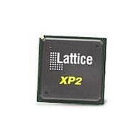
LFXP2-8E-7FT256C Lattice, LFXP2-8E-7FT256C Datasheet - Page 195

LFXP2-8E-7FT256C
Manufacturer Part Number
LFXP2-8E-7FT256C
Description
FPGA - Field Programmable Gate Array 8K LUTs 201I/O Inst- on DSP 1.2V -7 Spd
Manufacturer
Lattice
Datasheet
1.LFXP2-8E-5FTN256I.pdf
(341 pages)
Specifications of LFXP2-8E-7FT256C
Number Of Macrocells
8000
Number Of Programmable I/os
201
Data Ram Size
226304
Supply Voltage (max)
1.26 V
Maximum Operating Temperature
+ 85 C
Minimum Operating Temperature
0 C
Mounting Style
SMD/SMT
Supply Voltage (min)
1.14 V
Package / Case
FTBGA-256
Lead Free Status / RoHS Status
Lead free / RoHS Compliant
Available stocks
Company
Part Number
Manufacturer
Quantity
Price
Company:
Part Number:
LFXP2-8E-7FT256C
Manufacturer:
Lattice Semiconductor Corporation
Quantity:
10 000
- Current page: 195 of 341
- Download datasheet (10Mb)
Lattice Semiconductor
Figure 10-50. READ_ID Waveform
WRITE_EN (ACh)
The WRITE_EN command enables the TAG memory for programming. If the WRITE_EN command has not been
shifted into the device first, the PROGRAM_TAG, ERASE_TAG and STATUS commands do not take effect. This is
to prevent the TAG memory from erroneous erase or program.
The command is executed when the Chip Select pin is driven from low to high after the 24th dummy clock. Any
extra dummy clocks, if presented before driving the Chip Select pin to high, are ignored. After the Chip Select pin is
driven from low to high, a minimum of three clocks are required to complete the execution of the command.
The effect of this command is terminated by the WRITE_DIS command.
Figure 10-51. WRITE_EN Waveform
WRITE_DIS (78h)
The WRITE_DIS command disables the TAG memory for programming. It does not nullify the READ_TAG and
READ_ID commands.
The command is executed when the Chip Select pin is driven from low to high after the 24th dummy clock. Any
extra dummy clocks, if presented before driving the Chip Select pin to high, are ignored. After the Chip Select pin is
driven from low to high, a minimum of three clocks are required to complete the execution of the command.
CS
CLK
SI
SO
CS
CLK
SI
SO
8 Bits READ_ID
Command
Shifting Clocks
8 Command
3 Clocks To Initiate And Complete
24 Bits Dummy
HI-Z
Optional Extra Clocks
10-45
HIGH IMPEDANCE
0 1 2
32 Bits JTAG IDCODE
LatticeXP2 Memory Usage Guide
31
HI-Z
Related parts for LFXP2-8E-7FT256C
Image
Part Number
Description
Manufacturer
Datasheet
Request
R

Part Number:
Description:
FPGA - Field Programmable Gate Array 8K LUTs 201 I/O Inst on DSP 1.2V -5 Spd
Manufacturer:
Lattice
Datasheet:

Part Number:
Description:
FPGA - Field Programmable Gate Array 8K LUTs 201I/O Inst- on DSP 1.2V -5 Spd
Manufacturer:
Lattice
Datasheet:

Part Number:
Description:
FPGA - Field Programmable Gate Array 8K LUTs 100 I/O Inst on DSP 1.2V -5 Spd
Manufacturer:
Lattice
Datasheet:

Part Number:
Description:
FPGA - Field Programmable Gate Array 8K LUTs 100I/O Inst- on DSP 1.2V -5 Spd
Manufacturer:
Lattice
Datasheet:

Part Number:
Description:
IC, LATTICEXP2 FPGA, 435MHZ, QFP-208
Manufacturer:
LATTICE SEMICONDUCTOR
Datasheet:
Part Number:
Description:
FPGA LatticeXP2 Family 8000 Cells Flash Technology 1.2V 144-Pin TQFP
Manufacturer:
LATTICE SEMICONDUCTOR
Datasheet:

Part Number:
Description:
IC DSP 8KLUTS 146I/O 208PQFP
Manufacturer:
Lattice
Datasheet:

Part Number:
Description:
IC DSP 8KLUTS 100I/O 144TQFP
Manufacturer:
Lattice
Datasheet:

Part Number:
Description:
IC DSP 8KLUTS 86I/O 132CSBGA
Manufacturer:
Lattice
Datasheet:

Part Number:
Description:
IC DSP 8KLUTS 86I/O 132CSBGA
Manufacturer:
Lattice
Datasheet:

Part Number:
Description:
IC DSP 8KLUTS 146I/O 208PQFP
Manufacturer:
Lattice
Datasheet:

Part Number:
Description:
IC DSP 8KLUTS 201I/O 256FTBGA
Manufacturer:
Lattice
Datasheet:

Part Number:
Description:
IC FPGA 8KLUTS 86I/O 132-BGA
Manufacturer:
Lattice
Datasheet:

Part Number:
Description:
IC FPGA 8KLUTS 86I/O 132-BGA
Manufacturer:
Lattice
Datasheet:

Part Number:
Description:
IC FPGA 8KLUTS 201I/O 256-BGA
Manufacturer:
Lattice
Datasheet:


