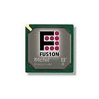
AFS600-FGG484 Actel, AFS600-FGG484 Datasheet - Page 156

AFS600-FGG484
Manufacturer Part Number
AFS600-FGG484
Description
FPGA - Field Programmable Gate Array 600K System Gates
Manufacturer
Actel
Datasheet
1.AFS600-PQG208.pdf
(330 pages)
Specifications of AFS600-FGG484
Processor Series
AFS600
Core
IP Core
Maximum Operating Frequency
1098.9 MHz
Number Of Programmable I/os
172
Data Ram Size
110592
Supply Voltage (max)
1.575 V
Maximum Operating Temperature
+ 70 C
Minimum Operating Temperature
0 C
Development Tools By Supplier
AFS-Eval-Kit, AFS-BRD600, FlashPro 3, FlashPro Lite, Silicon-Explorer II, Silicon-Sculptor 3, SI-EX-TCA
Mounting Style
SMD/SMT
Supply Voltage (min)
1.425 V
Number Of Gates
600 K
Package / Case
FPBGA-484
Lead Free Status / RoHS Status
Lead free / RoHS Compliant
Available stocks
Company
Part Number
Manufacturer
Quantity
Price
Company:
Part Number:
AFS600-FGG484
Manufacturer:
Actel
Quantity:
135
Company:
Part Number:
AFS600-FGG484I
Manufacturer:
Microsemi SoC
Quantity:
10 000
Part Number:
AFS600-FGG484I
Manufacturer:
MICROSEMI/美高森美
Quantity:
20 000
Company:
Part Number:
AFS600-FGG484K
Manufacturer:
Microsemi SoC
Quantity:
10 000
- Current page: 156 of 330
- Download datasheet (13Mb)
Device Architecture
Note:
Figure 2-98 • I/O Block Logical Representation
2- 14 0
From FPGA Core
Fusion I/Os have registers to support DDR functionality (see the
page 2-141
I/O Registers
Each I/O module contains several input, output, and enable registers. Refer to
simplified representation of the I/O block.
The number of input registers is selected by a set of switches (not shown in
registers to implement single or differential data transmission to and from the FPGA core. The Designer
software sets these switches for the user.
A common CLR/PRE signal is employed by all I/O registers when I/O register combining is used. Input
register 2 does not have a CLR/PRE pin, as this register is used for DDR implementation. The I/O
register combining must satisfy some rules.
for more information).
To FPGA Core
I/O / CLR or I/O / PRE / OCE
I/O / D1 / ICE
I/O / OCLK
I/O / ICLK
I/O / Q0
I/O / Q1
I/O / OE
I/O / D0
CLR/PRE
CLR/PRE
ICE
Input
Reg
Input
Reg
R e visio n 1
1
3
OCE
OCE
ICE
Enable
Output
Output
Output
Reg
Reg
Reg
6
4
5
CLR/PRE
CLR/PRE
CLR/PRE
"Double Data Rate (DDR) Support" section on
Input
Reg
2
A
Y
Resistor Control
Pull-Up/Down
E = Enable Pin
Figure
and Slew-Rate Control
PAD
Signal Drive Strength
Figure 2-98
2-98) between
for a
Related parts for AFS600-FGG484
Image
Part Number
Description
Manufacturer
Datasheet
Request
R

Part Number:
Description:
AFS600-1FGG256I
Manufacturer:
Actel
Datasheet:

Part Number:
Description:
AFS600-2FGG256I
Manufacturer:
Actel
Datasheet:


