MMA8452QR1 Freescale Semiconductor, MMA8452QR1 Datasheet - Page 11
MMA8452QR1
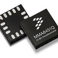
Manufacturer Part Number
MMA8452QR1
Description
Board Mount Accelerometers LOW G 3-AXIS 12BT EX VLT
Manufacturer
Freescale Semiconductor
Specifications of MMA8452QR1
Sensing Axis
X, Y, Z
Acceleration
2 g, 4 g, 8 g
Digital Output - Number Of Bits
8 bit, 12 bit
Supply Voltage (max)
3.6 V
Supply Voltage (min)
1.95 V
Maximum Operating Temperature
+ 85 C
Minimum Operating Temperature
- 40 C
Digital Output - Bus Interface
I2C
Shutdown
Yes
Sensitivity
256 count/g, 512 count/g, 1024 count/g
Package / Case
QFN-16
Output Type
Digital
Rohs Compliant
Yes
Peak Reflow Compatible (260 C)
Yes
Acceleration Range
± 2g, ± 4g, ± 8g
No. Of Axes
3
Ic Interface Type
I2C
Sensor Case Style
QFN
No. Of Pins
16
Supply Voltage Range
1.95V To 3.6V
Lead Free Status / RoHS Status
Lead free / RoHS Compliant
Available stocks
Company
Part Number
Manufacturer
Quantity
Price
Company:

Part Number:
MMA8452QR1
Manufacturer:
FTDI
Quantity:
1 200
Company:
Part Number:
MMA8452QR1
Manufacturer:
FREESCAL
Quantity:
5 963
Company:
Part Number:
MMA8452QR1
Manufacturer:
FREESCAL
Quantity:
1 000
Part Number:
MMA8452QR1
Manufacturer:
NXP/恩智浦
Quantity:
20 000


Table 4. I
1. All values referred to VIH (min) and VIL (max) levels.
2. t
3. The maximum t
4. t
5. t
6. A Fast mode I
7. Cb = total capacitance of one bus line in pF.
8. The maximum t
2.3
Sensors
Freescale Semiconductor
SCL Clock Frequency
Bus Free Time between STOP and START Condition
Repeated START Hold Time
Repeated START Set-up Time
STOP Condition Set-up Time
SDA Data Hold Time
SDA Valid Time
SDA Valid Acknowledge Time
SDA Set-up Time
SCL Clock Low Time
SCL Clock High Time
SDA and SCL Rise Time
SDA and SCL Fall Time
Pulse width of spikes on SDA and SCL that must be suppressed by input filter
Pull-up = 4.7 k
Pull-up = 4.7 k
Pull-up = 4.7 k
Pull-up = 1 k
Pull-up = 1 k
by a transition time.
automatically be the case if the device does not stretch the LOW period of the SCL signal. If such a device does stretch the LOW period of the
SCL signal, it must output the next data bit to the SDA line t
specification) before the SCL line is released. Also the acknowledge timing must meet this set-up time
This allows series protection resistors to be connected in between the SDA and the SCL pins and the SDA/SCL bus lines without exceeding
the maximum specified t
HD;DAT
VD;DAT
VD;ACK
= time for Data signal from SCL LOW to SDA output (HIGH or LOW, depending on which one is worse).
2
is the data hold time that is measured from the falling edge of SCL, applies to data in transmission and the acknowledge.
= time for Acknowledgement signal from SCL LOW to SDA output (HIGH or LOW, depending on which one is worse).
C Slave Timing Values
I
2
Ω,
Ω
C Interface Characteristic
Ω,
Ω,
Ω,
2
, Cb = 400 pF
(4)
C device can be used in a Standard mode I
HD;DAT
Cb = 20 pF
f
for the SDA and SCL bus lines is specified at 300 ns. The maximum fall time for the SDA output stage t
Cb = 20 pF
Cb = 40 pF
Cb = 400 pF
(2)
could be 3.45 μs and 0.9 μs for Standard mode and Fast mode, but must be less than the maximum of t
(7) (8)
f
.
(5)
Parameter
(1)
2
C system, but the requirement t
r
(max) + t
SU;DAT
= 1000 + 250 = 1250 ns (according to the Standard mode I
Symbol
t
t
t
t
t
t
t
HD;STA
SU;STA
SU;STO
HD;DAT
VD;DAT
VD;ACK
SU;DAT
t
t
t
f
HIGH
LOW
SCL
BUF
t
SP
t
t
r
f
SU;DAT
250 ns must then be met. This will
100
Min
1.3
0.6
0.6
0.6
4.7
50
0
0
0
0
0
4
(6)
I
2
C Fast Mode
Non-functional
2.250
0.9
0.9
1000
Max
4.50
f
100
750
300
50
is specified at 250 ns.
(3)
(3)
(3)
VD;DAT
MMA8452Q
or t
MHz
MHz
Unit
kHz
kHz
—
μs
μs
μs
μs
μs
μs
μs
ns
μs
μs
ns
ns
ns
VD;ACK
2
C
11
Related parts for MMA8452QR1
Image
Part Number
Description
Manufacturer
Datasheet
Request
R

Part Number:
Description:
Manufacturer:
Freescale Semiconductor, Inc
Datasheet:
Part Number:
Description:
Manufacturer:
Freescale Semiconductor, Inc
Datasheet:
Part Number:
Description:
Manufacturer:
Freescale Semiconductor, Inc
Datasheet:
Part Number:
Description:
Manufacturer:
Freescale Semiconductor, Inc
Datasheet:
Part Number:
Description:
Manufacturer:
Freescale Semiconductor, Inc
Datasheet:
Part Number:
Description:
Manufacturer:
Freescale Semiconductor, Inc
Datasheet:
Part Number:
Description:
Manufacturer:
Freescale Semiconductor, Inc
Datasheet:
Part Number:
Description:
Manufacturer:
Freescale Semiconductor, Inc
Datasheet:
Part Number:
Description:
Manufacturer:
Freescale Semiconductor, Inc
Datasheet:
Part Number:
Description:
Manufacturer:
Freescale Semiconductor, Inc
Datasheet:
Part Number:
Description:
Manufacturer:
Freescale Semiconductor, Inc
Datasheet:
Part Number:
Description:
Manufacturer:
Freescale Semiconductor, Inc
Datasheet:
Part Number:
Description:
Manufacturer:
Freescale Semiconductor, Inc
Datasheet:
Part Number:
Description:
Manufacturer:
Freescale Semiconductor, Inc
Datasheet:
Part Number:
Description:
Manufacturer:
Freescale Semiconductor, Inc
Datasheet: