FDMS7670AS Fairchild Semiconductor, FDMS7670AS Datasheet

MOSFET N-CH 30V SYNCFET POWER56

FDMS7670AS

Manufacturer Part Number
FDMS7670AS
Description
MOSFET N-CH 30V SYNCFET POWER56
Manufacturer
Fairchild Semiconductor
Series
PowerTrench®, SyncFET™r
Datasheet

Specifications of FDMS7670AS

Input Capacitance (ciss) @ Vds
4225pF @ 15V
Fet Type
MOSFET N-Channel, Metal Oxide
Fet Feature
Logic Level Gate
Rds On (max) @ Id, Vgs
3 mOhm @ 21A, 10V
Drain To Source Voltage (vdss)
30V
Current - Continuous Drain (id) @ 25° C
22A
Vgs(th) (max) @ Id
3V @ 1mA
Gate Charge (qg) @ Vgs
66nC @ 10V
Power - Max
2.5W
Mounting Type
Surface Mount
Package / Case
8-PQFN, Power56
Configuration
Single
Transistor Polarity
N-Channel
Resistance Drain-source Rds (on)
3 m Ohms
Forward Transconductance Gfs (max / Min)
300 S
Drain-source Breakdown Voltage
30 V
Continuous Drain Current
42 A
Power Dissipation
65 W
Maximum Operating Temperature
+ 150 C
Mounting Style
SMD/SMT
Minimum Operating Temperature
- 55 C
Lead Free Status / RoHS Status
Lead free / RoHS Compliant

Available stocks

Company
Part Number
Manufacturer
Quantity
Price
Part Number:
FDMS7670AS
Manufacturer:
FAIRCHILD/仙童
Quantity:
20 000
Company:
Part Number:
FDMS7670AS
Quantity:
32
©2010 Fairchild Semiconductor Corporation
FDMS7670AS Rev.C1
FDMS7670AS
N-Channel PowerTrench
30 V, 42 A, 3 m
Features
MOSFET Maximum Ratings
Thermal Characteristics
Package Marking and Ordering Information
V
V
I
dv/dt
E
P
T
R
R
D
DS
GS
AS
D
J
Max r
Max r
Advanced Package and Silicon combination for low r
and high efficiency
SyncFET Schottky Body Diode
MSL1 robust package design
100% UIL tested
RoHS Compliant
, T
JC
JA
Symbol
Device Marking
STG
FDMS7670AS
DS(on)
DS(on)
= 3.0 m at V
= 3.2 m at V
Top
Drain to Source Voltage
Gate to Source Voltage
Drain Current -Continuous (Package limited)
MOSFET dv/dt
Single Pulse Avalanche Energy
Power Dissipation
Power Dissipation
Operating and Storage Junction Temperature Range
Thermal Resistance, Junction to Case
Thermal Resistance, Junction to Ambient
GS
GS
FDMS7670AS
= 10 V, I
= 7 V, I
-Continuous
-Continuous (Silicon limited)
-Pulsed
Device
Power 56
D
D
= 19 A
= 21 A
T
®
C
D
= 25 °C unless otherwise noted
SyncFET
D
Parameter
D
D
Bottom
DS(on)
Power 56
Package
1
S
TM
T
T
T
S
T
T
General Description
The FDMS7670AS has been designed to minimize losses in
power conversion application. Advancements in both silicon and
package technologies have been combined to offer the lowest
r
device has the added benefit of an efficient monolithic Schottky
body diode.
Applications
C
C
A
C
A
DS(on)
S
= 25 °C
= 25 °C
= 25 °C
= 25 °C
= 25 °C
Synchronous Rectifier for DC/DC Converters
Notebook Vcore/ GPU low side switch
Networking Point of Load low side switch
Telecom secondary side rectification
Pin 1
G
while maintaining excellent switching performance. This
Reel Size
13 ’’
(Note 1a)
(Note 1a)
(Note 1a)
(Note 3)
(Note 4)
D
D
D
D
5
6
7
8
Tape Width
12 mm
-55 to +150
Ratings
±20
113
150
1.9
1.8
2.5
30
42
22
98
65
50
www.fairchildsemi.com
March 2010
3000 units
4
3
2
1
Quantity
G
S
S
S
Units
°C/W
V/ns
mJ
°C
W
V
V
A

Related parts for FDMS7670AS

FDMS7670AS Summary of contents

Page 1

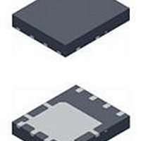
... Device FDMS7670AS FDMS7670AS ©2010 Fairchild Semiconductor Corporation FDMS7670AS Rev.C1 ® TM SyncFET General Description The FDMS7670AS has been designed to minimize losses power conversion application. Advancements in both silicon and = package technologies have been combined to offer the lowest r while maintaining excellent switching performance. This ...

Page 2

... JA the user's board design. 2. Pulse Test: Pulse Width < 300 s, Duty cycle < 2.0%. ° based on starting mH N-ch device, the negative Vgs rating is for low duty cycle pulse occurrence only. No continuous rating is implied. FDMS7670AS Rev. °C unless otherwise noted A Test Conditions mA mA, referenced to 25 °C ...

Page 3

... Figure 3. Normalized On- Resistance vs Junction Temperature 150 PULSE DURATION = 80 s DUTY CYCLE = 0.5% MAX 120 125 1.0 1.5 2.0 2 GATE TO SOURCE VOLTAGE (V) GS Figure 5. Transfer Characteristics FDMS7670AS Rev. °C unless otherwise noted PULSE DURATION = 80 s DUTY CYCLE = 0.5% MAX 1.5 2 100 125 150 - ...

Page 4

... Switching Capability 200 100 10 THIS AREA IS 1 LIMITED BY r DS(on) SINGLE PULSE T = MAX RATED 0 125 C 0.01 0.01 0 DRAIN to SOURCE VOLTAGE (V) DS Figure 11. Forward Bias Safe Operating Area FDMS7670AS Rev. °C unless otherwise noted J 5000 1000 120 100 100 300 10000 100 s 1000 ...

Page 5

... Typical Characteristics 2 1 DUTY CYCLE-DESCENDING ORDER D = 0.5 0.2 0.1 0.1 0.05 0.02 0.01 0.01 0.001 0.0001 - Figure 13. Junction-to-Ambient Transient Thermal Response Curve FDMS7670AS Rev. °C unless otherwise noted J SINGLE PULSE 125 C RECTANGULAR PULSE DURATION (sec NOTES: DUTY FACTOR PEAK 100 1 10 www ...

Page 6

... MOSFET. Figure 14 shows the reverses recovery characteristic of the FDMS7670AS di/dt = 300 TIME (ns) Figure 14. FDMS7670AS SyncFET body diode reverse recovery characteristic FDMS7670AS Rev.C1 (continued) Schottky barrier diodes exhibit significant leakage at high tem- perature and high reverse voltage. This will increase the power in the device ...

Page 7

... Dimensional Outline and Pad Layout FDMS7670AS Rev.C1 7 www.fairchildsemi.com ...

Page 8

... Datasheet Identification Product Status Advance Information Formative / In Design Preliminary First Production No Identification Needed Full Production Obsolete Not In Production FDMS7670AS Rev.C1 ® FRFET PowerTrench SM Global Power Resource PowerXS™ Green FPS™ Programmable Active Droop™ ® Green FPS™ e-Series™ ...

Related keywords