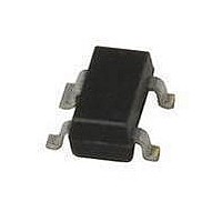
BFG505/X,235 NXP Semiconductors, BFG505/X,235 Datasheet - Page 3

BFG505/X,235
Manufacturer Part Number
BFG505/X,235
Description
TRANS RF NPN 9GHZ SOT4
Manufacturer
NXP Semiconductors
Datasheet
1.BFG505215.pdf
(13 pages)
Specifications of BFG505/X,235
Package / Case
TO-253-4, TO-253AA
Transistor Type
NPN
Voltage - Collector Emitter Breakdown (max)
15V
Frequency - Transition
9GHz
Noise Figure (db Typ @ F)
1.2dB ~ 2.1dB @ 900MHz
Power - Max
150mW
Dc Current Gain (hfe) (min) @ Ic, Vce
60 @ 5mA, 6V
Current - Collector (ic) (max)
18mA
Mounting Type
Surface Mount
Dc Collector/base Gain Hfe Min
60
Dc Current Gain Hfe Max
250
Mounting Style
SMD/SMT
Configuration
Single
Transistor Polarity
NPN
Collector- Emitter Voltage Vceo Max
15 V
Emitter- Base Voltage Vebo
2.5 V
Continuous Collector Current
18 mA
Power Dissipation
150 mW
Lead Free Status / RoHS Status
Lead free / RoHS Compliant
Gain
-
Lead Free Status / RoHS Status
Lead free / RoHS Compliant, Lead free / RoHS Compliant
NXP Semiconductors
LIMITING VALUES
In accordance with the Absolute Maximum System (IEC 134).
Note
1. T
THERMAL CHARACTERISTICS
Note
1. T
handbook, halfpage
V
V
V
I
P
T
T
R
SYMBOL
C
stg
j
CBO
CES
EBO
tot
th j-s
NPN 9 GHz wideband transistors
SYMBOL
(mW)
s
s
P tot
200
150
100
is the temperature at the soldering point of the collector pin.
is the temperature at the soldering point of the collector pin.
50
0
0
thermal resistance from junction to soldering point
Fig.2 Power derating curve.
collector-base voltage
collector-emitter voltage
emitter-base voltage
collector current (DC)
total power dissipation
storage temperature range
junction temperature
50
PARAMETER
100
PARAMETER
150
T s ( C)
MRA638-1
200
Rev. 04 - 22 November 2007
open emitter
R
open collector
T
s
BE
= 0
130 C; see Fig.2; note 1
CONDITIONS
note 1
CONDITIONS
BFG505; BFG505/X
65
MIN.
20
15
2.5
18
150
150
175
Product specification
VALUE
MAX.
290
3 of 13
V
V
V
mA
mW
C
C
UNIT
UNIT
K/W


