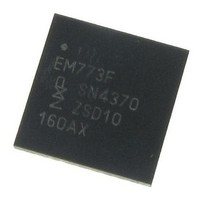
EM773FHN33,551 NXP Semiconductors, EM773FHN33,551 Datasheet - Page 17

EM773FHN33,551
Manufacturer Part Number
EM773FHN33,551
Description
IC ENERGY METER ARM 32VQFN
Manufacturer
NXP Semiconductors
Datasheet
1.EM773FHN33551.pdf
(45 pages)
Specifications of EM773FHN33,551
Core Processor
ARM Cortex-M0
Core Size
32-Bit
Speed
48MHz
Connectivity
I²C, SPI, UART/USART
Peripherals
Brown-out Detect/Reset, POR, WDT
Number Of I /o
25
Program Memory Size
32KB (32K x 8)
Program Memory Type
FLASH
Ram Size
8K x 8
Voltage - Supply (vcc/vdd)
1.8 V ~ 3.6 V
Oscillator Type
Internal
Operating Temperature
-40°C ~ 85°C
Package / Case
32-VQFN Exposed Pad
Output Voltage
3.6 V
Output Current
20 mA
Output Power
1.5 W
Input Voltage
1.8 V to 3.6 V
Switching Frequency
48 MHz
Operating Temperature Range
- 40 C to + 85 C
Mounting Style
SMD/SMT
Duty Cycle (max)
50 %
Number Of Outputs
10
Lead Free Status / RoHS Status
Lead free / RoHS Compliant
Eeprom Size
-
Data Converters
-
Lead Free Status / Rohs Status
Lead free / RoHS Compliant
Other names
568-5213
NXP Semiconductors
EM773
Objective data sheet
CAUTION
7.16.4 Code security (Code Read Protection - CRP)
7.16.5 APB interface
7.16.6 AHBLite
7.16.7 External interrupt inputs
7.17 Emulation and debugging
This feature of the EM773 allows user to enable different levels of security in the system
so that access to the on-chip flash and use of the Serial Wire Debugger (SWD) and
In-System Programming (ISP) can be restricted. When needed, CRP is invoked by
programming a specific pattern into a dedicated flash location. IAP commands are not
affected by the CRP.
In addition, ISP entry via the PIO0_1 pin can be disabled without enabling CRP. For
details see the EM773 user manual.
There are three levels of Code Read Protection:
In addition to the three CRP levels, sampling of pin PIO0_1 for valid user code can be
disabled. For details see the EM773 user manual.
The APB peripherals are located on one APB bus.
The AHBLite connects the CPU bus of the ARM Cortex-M0 to the flash memory, the main
static RAM, and the Boot ROM.
All GPIO pins can be level or edge sensitive interrupt inputs.
Debug functions are integrated into the ARM Cortex-M0. Serial wire debug with four
breakpoints and two watchpoints is supported.
1. CRP1 disables access to the chip via the SWD and allows partial flash update
2. CRP2 disables access to the chip via the SWD and only allows full flash erase and
3. Running an application with level CRP3 selected fully disables any access to the chip
(excluding flash sector 0) using a limited set of the ISP commands. This mode is
useful when CRP is required and flash field updates are needed but all sectors can
not be erased.
update using a reduced set of the ISP commands.
via the SWD pins and the ISP. This mode effectively disables ISP override using
PIO0_1 pin, too. It is up to the user’s application to provide (if needed) flash update
mechanism using IAP calls or call reinvoke ISP command to enable flash update via
the UART.
If level three Code Read Protection (CRP3) is selected, no future factory testing can be
performed on the device.
All information provided in this document is subject to legal disclaimers.
Rev. 1 — 1 September 2010
Energy metering IC
© NXP B.V. 2010. All rights reserved.
EM773
17 of 45


