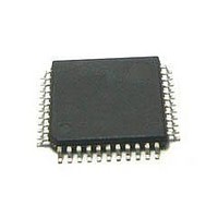
MC56F8255VLD Freescale Semiconductor, MC56F8255VLD Datasheet - Page 30

MC56F8255VLD
Manufacturer Part Number
MC56F8255VLD
Description
DSC 64K FLASH 60MHZ 44-LQFP
Manufacturer
Freescale Semiconductor
Series
56F8xxxr
Datasheets
1.TWR-56F8257.pdf
(88 pages)
2.MC56F8245VLD.pdf
(14 pages)
3.MC56F8245VLD.pdf
(2 pages)
4.MC56F8245VLD.pdf
(629 pages)
Specifications of MC56F8255VLD
Core Processor
56800E
Core Size
16-Bit
Speed
60MHz
Connectivity
CAN, I²C, LIN, SCI, SPI
Peripherals
LVD, POR, PWM, WDT
Number Of I /o
35
Program Memory Size
64KB (32K x 16)
Program Memory Type
FLASH
Ram Size
4K x 16
Voltage - Supply (vcc/vdd)
3 V ~ 3.6 V
Data Converters
A/D 8x12b, D/A 1x12b
Oscillator Type
Internal
Operating Temperature
-40°C ~ 105°C
Package / Case
44-LQFP
Product
DSCs
Processor Series
56800E
Core
56800E
Device Million Instructions Per Second
60 MIPs
Maximum Clock Frequency
60 MHz
Number Of Programmable I/os
35
Data Ram Size
8 KB
Operating Supply Voltage
3.3 V
Maximum Operating Temperature
+ 105 C
Mounting Style
SMD/SMT
Minimum Operating Temperature
- 40 C
On-chip Adc
12 bit, 4 Channel
Lead Free Status / RoHS Status
Lead free / RoHS Compliant
Eeprom Size
-
Lead Free Status / Rohs Status
Details
Available stocks
Company
Part Number
Manufacturer
Quantity
Price
Company:
Part Number:
MC56F8255VLD
Manufacturer:
Freescale Semiconductor
Quantity:
10 000
Memory Maps
4.2
The MC56F825x/MC56F824x series provide up to 64 KB on-chip flash memory. It primarily accesses through the program
memory buses (PAB; PDB). PAB is used to select program memory addresses; instruction fetches are performed over PDB.
Data can be read from and written to the program memory space through the primary data memory buses: CDBW for data write
and CDBR for data read. Access time for accessing the program memory space over the data memory buses is longer than for
accessing data memory space. The special MOVE instructions are provided to support these accesses. The benefit is that
non-time-critical constants or tables can be stored and accessed in program memory.
The program memory map appears in
30
On-Chip Memory
Program Flash
Unified RAM
(PFLASH)
(RAM)
1
2
All addresses are 16-bit word addresses.
This RAM is shared with data space starting at address X: 0x00 0000. See
Program Map
Begin/End Address
Begin/End Address
P: 0x1F FFFF
P: 0x1F FFFF
P: 0x00 8FFF
P: 0x00 7FFF
P: 0x00 8FFF
P: 0x00 7FFF
P: 0x00 8800
P: 0x00 8000
P: 0x00 0000
P: 0x00 8800
P: 0x00 8000
P: 0x00 2000
P: 0x00 2000
P: 0x00 0000
56F8245
56F8246
24K x 16
3K x 16
48 KB
6 KB
or
or
Table 7. Program Memory Map
Table 8. Program Memory Map
MC56F825x/MC56F824x Digital Signal Controller, Rev. 3
56F8247
24K x 16
4K x 16
48 KB
RESERVED
On-chip RAM
RESERVED
On-chip RAM
RESERVED
8 KB
• Internal program flash: 64 KB
• Interrupt vector table locates from 0x00 0000 to 0x00 0085
• COP reset address = 0x00 0002
• Boot location = 0x00 0000
• Internal program flash: 48 KB
• Interrupt vector table locates from 0x00 2000 to 0x00 2085
• COP reset address = 0x00 2002
• Boot location = 0x00 2000
Table
or
or
Table 6. Chip Memory Configurations
7,
Table 8,
56F8255
56F8256
56F8357
32K x 16
4K x 16
64 KB
8 KB
2
2
or
or
: 8 KB
: 8 KB
and
Table
Erase/program via flash interface unit and word writes to CDBW
Usable by the program and data memory spaces
1
9, depending on the device.
for 56F8255/56/57 at Reset
Memory Allocation
1
Memory Allocation
for 56F82447 at Reset
Use Restrictions
Figure
6.
Freescale Semiconductor


