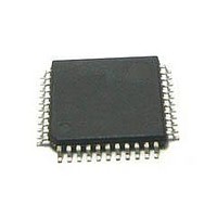
MC56F8255VLD Freescale Semiconductor, MC56F8255VLD Datasheet - Page 57

MC56F8255VLD
Manufacturer Part Number
MC56F8255VLD
Description
DSC 64K FLASH 60MHZ 44-LQFP
Manufacturer
Freescale Semiconductor
Series
56F8xxxr
Datasheets
1.TWR-56F8257.pdf
(88 pages)
2.MC56F8245VLD.pdf
(14 pages)
3.MC56F8245VLD.pdf
(2 pages)
4.MC56F8245VLD.pdf
(629 pages)
Specifications of MC56F8255VLD
Core Processor
56800E
Core Size
16-Bit
Speed
60MHz
Connectivity
CAN, I²C, LIN, SCI, SPI
Peripherals
LVD, POR, PWM, WDT
Number Of I /o
35
Program Memory Size
64KB (32K x 16)
Program Memory Type
FLASH
Ram Size
4K x 16
Voltage - Supply (vcc/vdd)
3 V ~ 3.6 V
Data Converters
A/D 8x12b, D/A 1x12b
Oscillator Type
Internal
Operating Temperature
-40°C ~ 105°C
Package / Case
44-LQFP
Product
DSCs
Processor Series
56800E
Core
56800E
Device Million Instructions Per Second
60 MIPs
Maximum Clock Frequency
60 MHz
Number Of Programmable I/os
35
Data Ram Size
8 KB
Operating Supply Voltage
3.3 V
Maximum Operating Temperature
+ 105 C
Mounting Style
SMD/SMT
Minimum Operating Temperature
- 40 C
On-chip Adc
12 bit, 4 Channel
Lead Free Status / RoHS Status
Lead free / RoHS Compliant
Eeprom Size
-
Lead Free Status / Rohs Status
Details
Available stocks
Company
Part Number
Manufacturer
Quantity
Price
Company:
Part Number:
MC56F8255VLD
Manufacturer:
Freescale Semiconductor
Quantity:
10 000
Figure 16
7.11
7.12
7.13
Freescale Semiconductor
1
2
3
NanoEdge Placement (NEP) step size
Delay for fault input activating to PWM output deactivated
Required: IP bus clock is between 50 MHz and ~60 Mhz in NanoEdge Placement mode.
NanoEdge Placement step size is a function of clock frequency only. Temperature and voltage variations do not affect
NanoEdge Placement step size.
In NanoEdge Placement mode, the minimum pulse edge-to-edge cannot be less than 4 PWM clock cycles.
•
•
•
•
1
2
Additional overhead is part of the programming sequence. Refer to the device’s reference manual for details.
Specifies page erase time. There are 1024 bytes per page in the program flash memory.
Frequency of operation (external clock driver)
Active state, when a bus or signal is driven, and enters a low impedance state
Tri-stated, when a bus or signal is placed in a high impedance state
Data Valid state, when a signal level has reached V
Data Invalid state, when a signal level is in transition between V
shows the definitions of the following signal states:
Enhanced Flex PWM Characteristics
Flash Memory Characteristics
External Clock Operation Timing
Data Invalid State
Mass erase time
Characteristic
Program time
Erase time
Data1 Valid
Clock pulse width
Data1
Characteristic
Characteristic
Table 29. External Clock Operation Timing Requirements
2
1
MC56F825x/MC56F824x Digital Signal Controller, Rev. 3
Table 27. Enhanced Flex PWM Timing Parameters
Data Active
1 2 3
3
Table 28. Flash Timing Parameters
Data2 Valid
Figure 16. Signal States
Symbol
t
Data2
t
erase
prog
t
me
2
Symbol
OL
f
t
osc
PW
or V
Symbol
Min
100
—
—
OH
20
20
Data
Three-stated
OL
6.25
Min
—
and V
Min
—
1
Typ
OH
—
—
—
Typ
—
—
Typ
521
—
Data3 Valid
Data Active
Data3
1
Max
40
—
—
Max
120
—
Max
—
Specifications
Unit
Unit
MHz
ms
ms
ns
s
Unit
ps
ns
57


