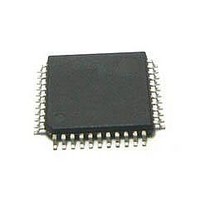
MC56F8255VLD Freescale Semiconductor, MC56F8255VLD Datasheet - Page 69

MC56F8255VLD
Manufacturer Part Number
MC56F8255VLD
Description
DSC 64K FLASH 60MHZ 44-LQFP
Manufacturer
Freescale Semiconductor
Series
56F8xxxr
Datasheets
1.TWR-56F8257.pdf
(88 pages)
2.MC56F8245VLD.pdf
(14 pages)
3.MC56F8245VLD.pdf
(2 pages)
4.MC56F8245VLD.pdf
(629 pages)
Specifications of MC56F8255VLD
Core Processor
56800E
Core Size
16-Bit
Speed
60MHz
Connectivity
CAN, I²C, LIN, SCI, SPI
Peripherals
LVD, POR, PWM, WDT
Number Of I /o
35
Program Memory Size
64KB (32K x 16)
Program Memory Type
FLASH
Ram Size
4K x 16
Voltage - Supply (vcc/vdd)
3 V ~ 3.6 V
Data Converters
A/D 8x12b, D/A 1x12b
Oscillator Type
Internal
Operating Temperature
-40°C ~ 105°C
Package / Case
44-LQFP
Product
DSCs
Processor Series
56800E
Core
56800E
Device Million Instructions Per Second
60 MIPs
Maximum Clock Frequency
60 MHz
Number Of Programmable I/os
35
Data Ram Size
8 KB
Operating Supply Voltage
3.3 V
Maximum Operating Temperature
+ 105 C
Mounting Style
SMD/SMT
Minimum Operating Temperature
- 40 C
On-chip Adc
12 bit, 4 Channel
Lead Free Status / RoHS Status
Lead free / RoHS Compliant
Eeprom Size
-
Lead Free Status / Rohs Status
Details
Available stocks
Company
Part Number
Manufacturer
Quantity
Price
Company:
Part Number:
MC56F8255VLD
Manufacturer:
Freescale Semiconductor
Quantity:
10 000
7.25.1
Figure 31
phases and operate at the ADC clock frequency. Equivalent input impedance, when the input is selected, is as follows:
where k =
and C
Freescale Semiconductor
1
2
3
4
5
6
7
8
9
Input impedance
AC Specifications
Signal-to-noise ratio
Total Harmonic Distortion
Spurious Free Dynamic Range
Signal-to-noise plus distortion
Effective Number Of Bits
Speed register setting must be 00 for ADC clock 5 MHz, 01 for 5 MHz < ADC clock 12 MHz, and 10 for ADC clock > 12 MHz
ADC PGA gain is x1
All measurements were made at V
Includes power-up of ADC and V
ADC clock cycles
INL and DNL measured from V
LSB = Least Significant Bit = 0.806 mV at x1 gain
Pin groups are detailed following
The current that can be injected or sourced from an unselected ADC signal input without affecting the performance of the ADC
Analog input
•
•
1.
gain
1 for first sample
6 for subsequent samples
Parasitic capacitance due to package, pin-to-pin, and pin-to-package base coupling: 1.8 pF
is as described in note 4 below.
illustrates the ADC input circuit during sample and hold. S1 and S2 are always opened/closed at non-overlapping
1
Equivalent Circuit for ADC Inputs
Parameter
9
2
(gain of 1x, 2x, 4x and f
(2 x k / ADCClockRate x C
125-ohm ESD
resisto
IN
MC56F825x/MC56F824x Digital Signal Controller, Rev. 3
REF
Table
= V
DD
3
r
REFL
= 3.3V, V
17.
Table 41. ADC Parameters
to V
equivalent resistance
IN
(V
ADC
REFH
REFHx
= V
Symbol
Channel Mux
SINAD
ENOB
SFDR
SNR
THD
100 ohms
X
REFH
= 3.3V, and V
IN
10 MHz)
- V
REFLx
gain
) / 2
4
) + 100 ohms + 125 ohms
Min
—
—
—
—
—
—
REFL
= ground
1
(continued)
S2
S1
S1
See
Figure 31
Typ
9.5
59
64
65
59
S2
C1
C1
C1: Single Ended Mode
2XC1: Differential Mode
C1: Single Ended Mode
2XC1: Differential Mode
S/H
Max
—
S1
S1
Specifications
Ohms
Unit
Bits
dB
dB
dB
dB
Eqn. 1
69


