LMK04000BEVAL/NOPB National Semiconductor, LMK04000BEVAL/NOPB Datasheet - Page 14
LMK04000BEVAL/NOPB
Manufacturer Part Number
LMK04000BEVAL/NOPB
Description
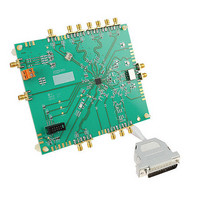
BOARD EVAL PRECISION CLOCK PLL
Manufacturer
National Semiconductor
Series
PowerWise®r
Datasheets
1.LMK04010BISQENOPB.pdf
(54 pages)
2.LMK04002BEVAL.pdf
(56 pages)
3.LMK04002BEVAL.pdf
(38 pages)
Specifications of LMK04000BEVAL/NOPB
Main Purpose
Timing, Clock Conditioner
Embedded
No
Utilized Ic / Part
LMK04000
Primary Attributes
122.88 MHz VCXO
Secondary Attributes
Integrated PLL & VCO
Lead Free Status / RoHS Status
Lead free / RoHS Compliant
Other names
LMK04000BEVAL
LMK04000BEVAL
LMK04000BEVAL


The following table contains descriptions of the various inputs and outputs for the evaluation board.
Table 6. LMK040XX Evaluation Board I/O
Connector Name
CLKin0/CLKin0*,
CLKin1/CLKin1*
LOS0, LOS1
CLKout0*,
CLKout1*,
CLKout2*,
CLKout3*,
CLKout0 /
CLKout1 /
CLKout2 /
CLKout3 /
CLKout4 /
CLKout4*
VccAux
Fout
Vcc
L M K 0 4 0 X X
Input/Output
Output
Output
Input
Input
Input
Output
Evaluation Board Inputs/Outputs
E V A L U A T I O N
number. If LVCMOS, each output can be independently configured
(non-inverted, inverted, tri-state, and LOW).
All clock outputs are AC-coupled.
configuration on the board contains a 3-dB attenuator on the Fout
signal.
DC power supply for the LMK040xx device.
Note: The LMK040xx family contains internal voltage regulators for the
VCO, PLL and related circuitry. The clock outputs do not have an
internal regulator. A clean power supply is required for best
performance.
Global Output Enable (GOE).
Notes:
setup for a single-ended reference source at CLKin0* (CLKin0 pin is
AC-coupled to ground). The format of the clock input buffer is
programmable in CodeLoader on the Bits/Pins tab, and may be either
bi-polar junction mode or MOS mode. The input power level for an AC-
coupled differential input should be between -2 dBm and +13 dBm for
bipolar mode and between +4 dBm and +13 dBm for MOS mode. If
either clock input is driven using a single-ended signal, the signal level
should be between -8 dBm and +8 dBm for bipolar mode, and between
-2 dBm and +10 dBm in MOS mode. If a DC-coupled clock is used to
drive either of the inputs, the peak voltage level must be at least 2 volts
and the minimum voltage no greater than 0.4 volts. By default CLKin0 is
the active input in either of the auto-switching modes (CLKin0 non-
revertive, CLKin0 revertive). When loss of CLKin0 is detected, the
device automatically switches to CLKin1 if an active reference clock is
attached. See data sheet for further explanation.
data sheet for further explanation of the LOS pins.
Description
Differential clock output pairs. See Table 1 for format depending on part
When enabled, buffered VCO output. AC-coupled. The default
DC power supply for on-board VCXOs, reference oscillators, and
Reference clock inputs for PLL1. The default board configuration is
Loss-of-Signal indicator (CMOS) for CLKin0/0* and CLKin1/1*. See
1. Vcc and VccAux power buses may be interconnected by
2. VCOs and VCXOs are sensitive to power supply noise. If the
placing a jumper on the VCC_TP header.
board is configured with and on-board VCXO or on-board
reference clock, best performance will be achieved if a clean
power supply is connected to VccAux.
14
B O A R D
O P E R A T I N G
I N S T R U C T I O N S
Related parts for LMK04000BEVAL/NOPB
Image
Part Number
Description
Manufacturer
Datasheet
Request
R

Part Number:
Description:
Low-noise Clock Jitter Cleaner With Cascaded Plls
Manufacturer:
National Semiconductor Corporation
Datasheet:
Part Number:
Description:
Lmk04000 Family Of Precision Clock Conditioners Low-noise Clock Jitter Cleaner With Cascaded Plls
Manufacturer:
National Semiconductor Corporation
Datasheet:

Part Number:
Description:
National Semiconductor [8-Bit D/A Converter]
Manufacturer:
National Semiconductor
Datasheet:
Part Number:
Description:
National Semiconductor [Media Coprocessor]
Manufacturer:
National Semiconductor
Datasheet:
Part Number:
Description:
Digitally Controlled Tone and Volume Circuit with Stereo Audio Power Amplifier, Microphone Preamp Stage and National 3D Sound
Manufacturer:
National Semiconductor
Datasheet:
Part Number:
Description:
Digitally Controlled Tone and Volume Circuit with Stereo Audio Power Amplifier, Microphone Preamp Stage and National 3D Sound
Manufacturer:
National Semiconductor
Datasheet:
Part Number:
Description:
AC97 Rev 2 Codec with Sample Rate Conversion and National 3D Sound
Manufacturer:
National Semiconductor
Part Number:
Description:
Manufacturer:
National Semiconductor
Datasheet:
Part Number:
Description:
Manufacturer:
National Semiconductor
Datasheet:
Part Number:
Description:
General Purpose, Low Voltage, Low Power, Rail-to-Rail Output Operational Amplifiers
Manufacturer:
National Semiconductor
Datasheet:
Part Number:
Description:
8-bit 20 MSPS flash A/D converter.
Manufacturer:
National Semiconductor
Datasheet:
Part Number:
Description:
Low Noise Quad Operational Amplifier
Manufacturer:
National Semiconductor
Datasheet:
Part Number:
Description:
Quad Differential Line Receivers
Manufacturer:
National Semiconductor
Datasheet:
Part Number:
Description:
Quad High Speed Trapezoidal? Bus Transceiver
Manufacturer:
National Semiconductor
Datasheet: