LMK04000BEVAL/NOPB National Semiconductor, LMK04000BEVAL/NOPB Datasheet - Page 8
LMK04000BEVAL/NOPB
Manufacturer Part Number
LMK04000BEVAL/NOPB
Description
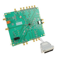
BOARD EVAL PRECISION CLOCK PLL
Manufacturer
National Semiconductor
Series
PowerWise®r
Datasheets
1.LMK04010BISQENOPB.pdf
(54 pages)
2.LMK04002BEVAL.pdf
(56 pages)
3.LMK04002BEVAL.pdf
(38 pages)
Specifications of LMK04000BEVAL/NOPB
Main Purpose
Timing, Clock Conditioner
Embedded
No
Utilized Ic / Part
LMK04000
Primary Attributes
122.88 MHz VCXO
Secondary Attributes
Integrated PLL & VCO
Lead Free Status / RoHS Status
Lead free / RoHS Compliant
Other names
LMK04000BEVAL
LMK04000BEVAL
LMK04000BEVAL


PLL Loop Filters and Loop Parameters
In jitter cleaning applications that use a cascaded PLL architecture, the first PLL affectively substitutes the
phase noise of a low noise oscillator (VCXO or crystal resonator) for the phase noise of a “dirty” reference
clock. The first PLL is typically configured with a narrow loop bandwidth in order to minimize the impact of
the reference clock phase noise. The reference clock consequently serves only as a frequency reference
rather than a phase reference. If the jitter of the VCXO is superior to that of the reference clock, the loop
bandwidth of the second PLL can be made much wider relative to the first PLL.
The loop filters on the LMK040xx evaluation board are setup using this approach. The loop filter for PLL1
has been configured for a narrow loop bandwidth (< 100 Hz), while the loop filter of PLL2 has been
configured for a wide loop bandwidth (> 50 kHz). The specific loop bandwidth values depend on the
phase noise performance of the oscillator mounted on the board. The following tables contain the
parameters for PLL1 and PLL2 for each oscillator option. National’s Clock Design Tool can be used to
optimize PLL phase noise/jitter for given specifications. For more information, please visit:
http://www.national.com/analog/timing/codeloader
Table 2. PLL1 and PLL2 Parameters for Crystal Mode operating with a 12.288 MHz XTAL.
Note: PLL Loop Bandwidth is a function of Kφ, Kvco, N as well as loop components. Changing Kφ and N will
change the loop bandwidth.
Ref Clk Frequency
Crystal Frequency
Loop Bandwidth
Loop Bandwidth
Supply Voltage
Supply Voltage
Phase Margin
Phase Margin
Components
Components
C3 = 100 pF
Loop Filter
Loop Filter
L M K 0 4 0 X X
XTAL OSC Option PLL 1 Loop Filter
C1 = 330 nF
(From PLL1)
C4 = 110 pF
XTAL Option PLL 2 Loop Filter
122.88 MHz
12.228 MHz
3.3 Volts
3.3 Volts
54 kHz
C1 = 0
10 Hz
E V A L U A T I O N
61º
66º
Output Frequency
Output Frequency
R3 = 0.6k ohms
C2 = 6.8 nF
B O A R D
C2 = 10 uF
VCO Gain
VCO Gain
8
Fcomp
Fcomp
Kφ
Kφ
O P E R A T I N G
I N S T R U C T I O N S
R2 = 3.9k ohms
R2 = 2.7k ohms
R4 = 0.2k ohms
1474.56 MHz
10 MHz/Volt
12.288 MHz
1.5 kHz/Volt
12.288 MHz
(To PLL 2)
1024 kHz
1600 uA
100 uA
Related parts for LMK04000BEVAL/NOPB
Image
Part Number
Description
Manufacturer
Datasheet
Request
R

Part Number:
Description:
Low-noise Clock Jitter Cleaner With Cascaded Plls
Manufacturer:
National Semiconductor Corporation
Datasheet:
Part Number:
Description:
Lmk04000 Family Of Precision Clock Conditioners Low-noise Clock Jitter Cleaner With Cascaded Plls
Manufacturer:
National Semiconductor Corporation
Datasheet:

Part Number:
Description:
National Semiconductor [8-Bit D/A Converter]
Manufacturer:
National Semiconductor
Datasheet:
Part Number:
Description:
National Semiconductor [Media Coprocessor]
Manufacturer:
National Semiconductor
Datasheet:
Part Number:
Description:
Digitally Controlled Tone and Volume Circuit with Stereo Audio Power Amplifier, Microphone Preamp Stage and National 3D Sound
Manufacturer:
National Semiconductor
Datasheet:
Part Number:
Description:
Digitally Controlled Tone and Volume Circuit with Stereo Audio Power Amplifier, Microphone Preamp Stage and National 3D Sound
Manufacturer:
National Semiconductor
Datasheet:
Part Number:
Description:
AC97 Rev 2 Codec with Sample Rate Conversion and National 3D Sound
Manufacturer:
National Semiconductor
Part Number:
Description:
Manufacturer:
National Semiconductor
Datasheet:
Part Number:
Description:
Manufacturer:
National Semiconductor
Datasheet:
Part Number:
Description:
General Purpose, Low Voltage, Low Power, Rail-to-Rail Output Operational Amplifiers
Manufacturer:
National Semiconductor
Datasheet:
Part Number:
Description:
8-bit 20 MSPS flash A/D converter.
Manufacturer:
National Semiconductor
Datasheet:
Part Number:
Description:
Low Noise Quad Operational Amplifier
Manufacturer:
National Semiconductor
Datasheet:
Part Number:
Description:
Quad Differential Line Receivers
Manufacturer:
National Semiconductor
Datasheet:
Part Number:
Description:
Quad High Speed Trapezoidal? Bus Transceiver
Manufacturer:
National Semiconductor
Datasheet: