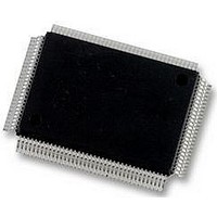
DP83865DVH National Semiconductor, DP83865DVH Datasheet - Page 10

DP83865DVH
Manufacturer Part Number
DP83865DVH
Description
10/100/1000BASE-T TRANSCEIVER, SMD
Manufacturer
National Semiconductor
Specifications of DP83865DVH
Data Rate
1000Mbps
No. Of Ports
1
Ethernet Type
IEEE 802.3u, IEEE 802.3z
Supply Current
430µA
Supply Voltage Range
2.375V To 2.625V, 3.135V To 3.465V
Operating Temperature Range
0°C To +70°C
Interface Type
GMII, MII, RGMII
Rohs Compliant
Yes
Leaded Process Compatible
No
Peak Reflow Compatible (260 C)
No
Lead Free Status / RoHS Status
Lead free / RoHS Compliant
Available stocks
Company
Part Number
Manufacturer
Quantity
Price
Company:
Part Number:
DP83865DVH
Manufacturer:
Texas Instruments
Quantity:
10 000
Company:
Part Number:
DP83865DVH/NOPB
Manufacturer:
NXP
Quantity:
1 000
Company:
Part Number:
DP83865DVH/NOPB
Manufacturer:
Texas Instruments
Quantity:
10 000
www.national.com
1.0 Pin Description
1.7 Reset
DUPLEX_LED /
PHYADDR0_STRAP
PHYADDR1_STRAP
PHYADDR2_STRAP
PHYADDR3_STRAP
PHYADDR4_STRAP
MULTI_EN_STRAP /
TX_TRIGGER
MDIX_EN_STRAP
MAC_CLK_EN_STRAP
/ TX_SYN_CLK
VDD_SEL_STRAP
RESET
Signal Name
Signal Name
I/O,
S, PU
PD
PD
PD
PD
I/O,
S, PD
I/O,
S, PU
I/O, S
Type
Type
I, S,
PU
(Continued)
I
PQFP
PQFP
Pin #
Pin #
13
14
17
18
95
94
89
88
34
33
PHY ADDRESS [4:0]: The DP83865 provides five PHY address-sensing pins
for multiple PHY applications. The setting on these five pins provides the base
address of the PHY.
The five PHYAD[4:0] bits are registered as inputs at reset with PHYADDR4 be-
ing the MSB of the 5-bit PHY address.
Note: The status of these bit is reflected in bits 4:0 of register 0x12.
DUPLEX STATUS: The LED is lit when the PHY is in Full Duplex operation
after the link is established.
MULTIPLE NODE ENABLE: This pin determines if the PHY advertises Master
(multiple nodes) or Slave (single node) priority during 1000BASE-T Auto-Ne-
gotiation.
‘1’ Selects multiple node priority (switch or hub)
‘0’ Selects single node priority (NIC)
Note: The status of this bit is reflected in bit 5 of register 0x10.
TX_TRIGGER: This output can be enabled during the IEEE 1000BASE-T test-
modes. This signal is not required by IEEE to perform the tests, but will help to
take measurements. TX_TRIGGER is only available in test modes 1 and 4 and
provides a trigger to allow for viewing test waveforms on an oscilloscope.
AUTO MDIX ENABLE: This pin controls the automatic pair swap (Auto-MDIX)
of the MDI/MDIX interface.
‘1’ enables pair swap mode
‘0’ disables the Auto-MDIX and defaults the part into the mode preset by the
MAN_MDIX_STRAP pin.
Note: The status of this bit is reflected in bit 6 of register 0x10. This pin also
sets the default for and can be overwritten by bit 15 of register 0x12.
CLOCK TO MAC ENABLE:
‘1’ CLK_TO_MAC clock output enabled
‘0’ CLK_TO_MAC disabled
Note: This status of this pin is reflected in bit 7 of register 0x10.
TX_SYN_CLK: This output can be enabled during the IEEE 1000BASE-T test-
modes. This signal is not required by IEEE to perform the tests, but will help to
take measurements. TX_SYN_CLK is only available in test modes 1 and 4.
TX_SYN_CLK = TX_TCLK / 4 in test mode 1
TX_SYN_CLK = TX_TCLK / 6 in test mode 4
IO_VDD SELECT: This pin selects between 2.5V or 3.3V for I/O VDD .
‘1’ selects 3.3V mode
‘0’ selects 2.5V mode
This pin must either be connected directly to ground or directly to a supply volt-
age (2.5V to 3.3V).
RESET: The active low RESET input allows for hard-reset, soft-reset, and TRI-
STATE output reset combinations. The RESET input must be low for a mini-
mum of 150 s.
10
Description
Description


