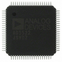
AD5522JSVDZ Analog Devices Inc, AD5522JSVDZ Datasheet - Page 16

AD5522JSVDZ
Manufacturer Part Number
AD5522JSVDZ
Description
IC, DAC, 16BIT, QFP-80
Manufacturer
Analog Devices Inc
Datasheet
1.AD5522JSVDZ.pdf
(64 pages)
Specifications of AD5522JSVDZ
Resolution (bits)
16bit
Input Channel Type
Serial
Supply Voltage Range - Digital
2.3V To 5.25V
Supply Current
36mA
Digital Ic Case Style
QFP
No. Of Pins
80
Data Interface
LVDS, Serial
Design Resources
Parametric Measurement Unit and Supporting Components for PAD Appls Using AD5522 and AD7685 (CN0104)
Lead Free Status / RoHS Status
Lead free / RoHS Compliant
Available stocks
Company
Part Number
Manufacturer
Quantity
Price
Company:
Part Number:
AD5522JSVDZ
Manufacturer:
WD
Quantity:
1 000
Company:
Part Number:
AD5522JSVDZ
Manufacturer:
Analog Devices Inc
Quantity:
10 000
Part Number:
AD5522JSVDZ
Manufacturer:
ADI/亚德诺
Quantity:
20 000
AD5522
PIN CONFIGURATIONS AND FUNCTION DESCRIPTIONS
Table 6. Pin Function Descriptions
Pin No.
1, 20, 41,
60, 74
2
3
4
5
6
7
8
9
10, 11, 50,
51, 69
12
Mnemonic
Exposed pad
AVDD
CFF0
CCOMP0
EXTMEASIH0
EXTMEASIL0
FOH0
GUARD0
GUARDIN0/
DUTGND0
MEASVH0
AGND
MEASVH2
NOTES
1. THE EXPOSED PAD IS INTERNALLY ELECTRICALLY CONNECTED TO AVSS. FOR ENHANCED THERMAL, ELECTRICAL,
GUARDIN0/DUTGND0
GUARDIN2/DUTGND2
AND BOARD LEVEL PERFORMANCE, THE EXPOSED PADDLE ON THE BOTTOM OF THE PACKAGE SHOULD BE SOLDERED
TO A CORRESPONDING THERMAL LAND PADDLE ON THE PCB.
EXTMEASIH0
EXTMEASIH2
EXTMEASIL0
EXTMEASIL2
Description
Positive Analog Supply Voltage.
Compensation Capacitor Input for Channel 0. See the Compensation Capacitors section.
Sense Input (High Sense) for High Current Range (Channel 0).
Sense Input (Low Sense) for High Current Range (Channel 0).
Guard Output Drive for Channel 0.
DUT Voltage Sense Input (High Sense) for Channel 0.
Analog Ground. These pins are the reference points for the analog supplies and the measure circuitry.
DUT Voltage Sense Input (High Sense) for Channel 2.
The exposed pad is internally electrically connected to AVSS. For enhanced thermal, electrical, and board level
performance, the exposed paddle on the bottom of the package should be soldered to a corresponding
thermal land paddle on the PCB.
External Capacitor for Channel 0. This pin optimizes the stability and settling time performance of the force
amplifier when in force voltage mode. See the Compensation Capacitors section.
Force Output for Internal Current Ranges (Channel 0).
Guard Amplifier Input for Channel 0/DUTGND Input for Channel 0. This dual function pin is configured via the
serial interface. The default function at power-on is GUARDIN0. If this pin is configured as a DUTGND input for
the channel, the input to the guard amplifier is internally connected to MEASVH0. For more information, see
the Device Under Test Ground (DUTGND) section and the Guard Amplifier section.
MEASVH0
MEASVH2
CCOMP0
CCOMP2
GUARD0
GUARD2
AGND
AGND
AVDD
AVDD
FOH0
FOH2
CFF0
CFF2
10
12
13
14
16
17
19
20
11
15
18
1
4
2
3
5
6
7
8
9
21 22 23 24 25 26 27 28 29 30 31 32 33 34 35 36 37 38 39 40
80
PIN 1
79
Figure 8. Pin Configuration, Exposed Pad on Bottom
78
77
76
75
EXPOSED PAD ON BOTTOM
74
Rev. D | Page 16 of 64
73
(Not to Scale)
AD5522
TOP VIEW
72
71
70
69
68
67
66
65
64
63
62
61
60
59
58
57
56
55
54
53
52
51
50
49
48
47
46
45
44
43
42
41
AVDD
CFF1
CCOMP1
EXTMEASIH1
EXTMEASIL1
FOH1
GUARD1
GUARDIN1/DUTGND1
MEASVH1
AGND
AGND
MEASVH3
GUARDIN3/DUTGND3
GUARD3
FOH3
EXTMEASIL3
EXTMEASIH3
CCOMP3
CFF3
AVDD


