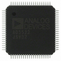
AD5522JSVDZ Analog Devices Inc, AD5522JSVDZ Datasheet - Page 34

AD5522JSVDZ
Manufacturer Part Number
AD5522JSVDZ
Description
IC, DAC, 16BIT, QFP-80
Manufacturer
Analog Devices Inc
Datasheet
1.AD5522JSVDZ.pdf
(64 pages)
Specifications of AD5522JSVDZ
Resolution (bits)
16bit
Input Channel Type
Serial
Supply Voltage Range - Digital
2.3V To 5.25V
Supply Current
36mA
Digital Ic Case Style
QFP
No. Of Pins
80
Data Interface
LVDS, Serial
Design Resources
Parametric Measurement Unit and Supporting Components for PAD Appls Using AD5522 and AD7685 (CN0104)
Lead Free Status / RoHS Status
Lead free / RoHS Compliant
Available stocks
Company
Part Number
Manufacturer
Quantity
Price
Company:
Part Number:
AD5522JSVDZ
Manufacturer:
WD
Quantity:
1 000
Company:
Part Number:
AD5522JSVDZ
Manufacturer:
Analog Devices Inc
Quantity:
10 000
Part Number:
AD5522JSVDZ
Manufacturer:
ADI/亚德诺
Quantity:
20 000
AD5522
When configured as DUTGND per channel, this dual function
pin is no longer connected to the input of the guard amplifier.
Instead, it is connected to the low end of the instrumentation
amplifier (SW14a), and the input of the guard amplifier is
connected internally to MEASVHx (SW13a).
GUARD AMPLIFIER
A guard amplifier allows the user to bootstrap the shield of
the cable to the voltage applied to the DUT, ensuring minimal
drops across the cable. This is particularly important for
measurements requiring a high degree of accuracy and in leakage
current testing.
If not required, all four guard amplifiers can be disabled via the
serial interface (system control register). Disabling the guard
amplifiers decreases power consumption by 400 μA per channel.
As described in the Device Under Test Ground (DUTGND)
section, GUARDINx/DUTGNDx are dual function pins. Each
pin can function either as a guard amplifier input for one chan-
nel or as a DUTGND input for one channel, depending on the
requirements of the end application (see Figure 49).
A guard alarm event occurs when the guard output moves more
than 100 mV away from the guard input voltage for more than
200 μs. In this case, the event is flagged via the open-drain output
CGALM . Because the guard and clamp alarm functions share
the same alarm output, CGALM , the alarm information (alarm
trigger and alarm channel) is available via the serial interface in
the alarm status register.
Alternatively, the serial interface allows the user to set up the
CGALM output to flag either the clamp status or the guard
status. By default, this open-drain alarm pin is an unlatched
output, but it can be configured as a latched output via the serial
interface (system control register).
AGND
x1
+
–
MEASURE
VOLTAGE
Figure 49. Using the DUTGND per Channel Feature
IN-AMP
+
–
SW14
+
–
a
b
SW13
b
a
GUARD
AMP
GUARDIN[0:3]/
MEASVH[0:3]
DUTGND[0:3]
GUARD[0:3]
SW16
DUTGND
DUT
Rev. D | Page 34 of 64
COMPENSATION CAPACITORS
Each channel requires an external compensation capacitor
(CCOMP) to ensure stability into the maximum load capacitance
while ensuring that settling time is optimized. In addition, one
CFF pin per channel is provided to further optimize stability and
settling time performance when in force voltage (FV) mode. When
changing from force current (FI) mode to FV mode, the internal
switch connecting the CFF capacitor is automatically closed.
Although the force amplifier is designed to drive load capacitances
up to 10 nF (with CCOMP capacitor = 100 pF), it is possible to
use larger compensation capacitor values to drive larger loads,
at the expense of an increase in settling time. If a wide range of
load capacitances must be driven, an external multiplexer
connected to the CCOMPx pin allows optimization of settling
time vs. stability. The series resistance of a switch placed on
CCOMPx should typically be <50 Ω.
Suitable multiplexers for use are the ADG1404, ADG1408, or
one of the multiplexers in the ADG4xx family, which typically
have on resistances of less than 50 Ω.
Similarly, connecting the CFF node to an external multiplexer
accommodates a wide range of C
or
The series resistance of the multiplexer used should be such that
The voltage range of the CFFx and CCOMPx pins is the same as
the voltage range expected on the FOHx pin; therefore, choice
of capacitor must take this into account.
Table 12. Suggested Compensation Capacitor Selection
C
≤1 nF
≤10 nF
≤100 nF
LOAD
ADG1209
1/(2π × R
family of multiplexers meet these requirements.
ON
× C
DUT
CCOMP Capacitor
100 pF
100 pF
C
) > 100 kHz
LOAD
/100
DUT
in FV mode. The
CFF Capacitor
C
220 pF
1 nF
LOAD
/10
ADG1204


